Photovoltaics
Photovoltaic (PV) materials and devices play a crucial role in our fight to reduce human-made greenhouse gas emissions. However, fossil fuel-derived electricity is still cheaper to produce (typically) than electricity from renewable sources like PV. To make (or, in some cases, keep) renewable electricity cost-competitive with fossil fuel electricity, we must continue to improve PV and other renewable technologies.
Cathodoluminescence (CL) is useful for revealing the microscopic mechanisms that determine the macroscopic performance of PV devices and modules. This allows researchers to understand and analyze fundamental physical and chemical processes in materials such as thin-film, perovskite, silicon, and other semiconductors; industrial applications include quality control and failure analysis.
Thin-film Multi-crystalline silicon
Perovskites
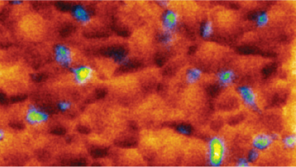
Despite only recently becoming an intense research focus, halide perovskite solar cells achieve exceptional efficiencies that surpass thin-film PV materials like CdTe and CuInGaSe2. They exhibit high carrier mobility, long diffusion lengths, and tunable spectral absorption windows. As a result, many researchers claim halide perovskites have the potential to be the most extraordinary and market-competitive optoelectronic material. With that in mind, significant hurdles remain to mainstream adoption, and researchers will require characterization techniques capable of exposing the interplay among structure, chemistry, and optoelectronic properties to inform processing strategies to increase device efficiencies and long‐term stability.
CL microscopy is an ideal technique for providing this type of information due to its ability to capture high spatial resolution and robust optical and electronic information. CL can monitor degradation due to environmental factors, reveal phase segregation resulting from material processing, and address other halide perovskite‐centric material issues.
It was once thought that electron beam‐based analysis of halide perovskites was impractical due to the instability of material properties when exposed to high-energy electrons. However, recent developments have stabilized formulations and refined optical designs for high sensitivity and repeatability, making analysis below the damage threshold for many halide perovskites possible.
Experimental brief
 |
Revealing the spatial distribution of phases in perovskite solar cells for the development of high efficiency and stable devices |
Thin-film
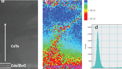
Thin-film solar cells based on CdTe or CIGS are the leading PV technology widely commercialized. Further improvements to device and module efficiencies require increased minority-carrier lifetime within the CdTe absorber layer. The low minority-carrier lifetime in polycrystalline thin films is thought to be caused by non-radiative Shockley-Read-Hall (SRH) recombination at deep levels in the band gap created by crystal defects—both point defects and extended defects are known to be prevalent in thin-film solar cells. However, there has been a failure to reach a consensus on precisely which defect(s) is(are) most limiting with the ongoing debate surrounding the role of grain boundaries after thermal processing. To this end, cathodoluminescence (CL) is an important technique that enables researchers to analyze recombination processes at the defect scale, allowing macroscale device performance to be understood from the microscopic behavior.
Many researchers use the nano-scale spatial resolution of CL to qualitatively and quantitatively compare carrier recombination and defects at grain boundaries and interiors before and after treatments designed to passivate defects. The contrast in a CL map of a polycrystalline material reveals regions of the specimen with strong(er) non-radiative SRH recombination, often grain boundaries. Statistical analysis and correlation using grain boundaries (e.g., EBSD analysis) provide a quantitative understanding of recombination at grain interiors and a variety of grain boundary types. Recently, CL measurements also allowed researchers to determine the grain boundary recombination velocity. Furthermore, capturing a complete CL spectrum at every (spatial) pixel in a map (spectrum imaging or hyperspectral imaging) allows researchers to map compositional variation within the compound semiconductor grain interiors and to develop more accurate band model diagrams to model carrier behavior.
Experimental brief
 |
Mapping the electronic bandgap of semiconductor compounds with milli-electron volt accuracy |
Multi-crystalline silicon
Silicon has an indirect electronic band structure. Since this band-to-band radiative recombination has only a low probability in comparison to non-radiative transitions at room temperature, it makes CL largely impractical. However, CL is useful for measuring the luminescence behavior of extended defects at cryogenic temperatures. These valuable measurements can simultaneously obtain spectrally and spatially resolved information to provide deep insights into the electronic structure of extended defects. For example, defects include dislocations and grain boundaries, which control the performance of many electronic and photovoltaic devices.
In many CL experiments, extended defects act as non-radiative recombination centers, and, therefore, the luminescence from band-band-recombination is decreased in the vicinity of extended defects compared to the undisturbed semiconductor. In the case of Si, Ge, and some compound semiconductor materials, dislocations and grain boundaries can exhibit characteristic luminescence bands (with photon energies lower than the band gap) that reveal the detailed electronic structure of defects. This allows researchers to develop accurate recombination models to improve device performance. Extensive CL investigations of bonded silicon wafers and multi-crystalline silicon show that dislocations and low-angle grain boundaries are responsible for the occurrence of shallow and deep levels in the band gap—the radiative transitions associated with these defect states are denoted as D-lines (D1 – D4). There remains ambiguity over the role of the strain field accompanying extended defects and oxygen and transition metal contamination. The correlation of the information revealed by CL with other techniques in the SEM, such as EBSD, shows strong promise as a means to resolve uncertainties and provide manufacturers guidance in optimizing materials and device processing.