Ceramics, Oxides, & Nitrides
Oxides, nitrides, and other ceramics are typically wide band gap materials regarded as insulators. These materials, like sapphire (Al2O3) and gallium oxide (Ga2O3), contain various point and structural defects and impurities. These defects and impurities provide a mechanism for the production of cathodoluminescence as free carriers generated by the electron beam recombine via the energy states inserted into the crystal's forbidden band gap. By characterizing the radiative recombination of electron beam excited electron-hole pairs, cathodoluminescence can reveal the presence and type of defects or impurities present and the material phase.
 |
Spectroscopic analysis of ultra-wide bandgap semiconductors |
Phosphors
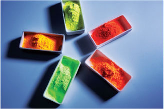
Phosphors are in myriad applications, including biofluorescent labels, display devices, plus LED and light bulb coatings. Phosphors emit brightly relative to other materials and present a different apparent color depending on their composition. Cathodoluminescence (CL) in the electron microscope is an ideal technique for evaluating phosphor luminescence because interaction with the focused electron beam can generate luminescence signals from individual phosphor particles, even those as small as a few nanometers in size, to allow investigation of variations between phosphor particles.
CL spectroscopy helps analyze many different phosphors, including individual nanometer-sized crystals of Y1.98Tb0.02O2S and Gd1.98Tb0.02O2S. In those studies, photon emission maps demonstrate a high degree of uniformity. Spectra from the two materials also show an identical intensity ratio between the 5D3 → 7FJ and 5D4 → 7FJ transitions, which is important evidence that the concentration of (activated) Tb3+ cations is very similar in these different crystals. Other researchers are developing these nanometer-sized phosphors as stable biological labels under electron beam illumination.
Oxides & Nitrides
 Oxides and nitrides, such as sapphire (Al2O3) and gallium oxide (Ga2O3), are considered wide band gap insulators. In these materials, the high-energy electron beam of an electron microscope offers an ideal tool to study the electronic and optical properties without resorting to specialized deep ultraviolet lasers for photoluminescence. Cathodoluminescence (CL) helps determine the energy band gap and reveal the presence (and energy state) of electrically active defects. This makes it a preferred tool to study the basic optical properties of these materials and discriminate between different phases of compositionally and chemically identical materials, e.g., the anatase and rutile phases of TiO2.
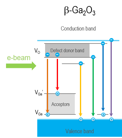
Recently, β-Ga2O3 has received increased attention due to its intrinsic ultra-wide band gap and optical transparency in visible light, implying a natural application to solar-blind ultraviolet (UV) photodetection. Limited techniques exist to determine material quality and characterize the defects that may be present. CL is one such technique—CL spectroscopy has been used to reveal oxygen vacancy-related and (two) gallium vacancy-related energy levels within the β-Ga2O3 band gap, including spectral changes associated with removing or creating these defects through materials processing. These defect levels compete with the near band edge luminescence, and the relative ratio of the two luminescence types provides insight into material quality.
|
|
Spectroscopic analysis of ultra-wide bandgap semiconductors |
Dielectric Materials
Dielectric materials are technologically important in the semiconductor industry. They are used as gate oxides in metal oxide semiconductor field effect (MOSFET) transistors. Silicon dioxide and silicon nitride are studied extensively using cathodoluminescence (CL) to characterize point defect clusters' structure and electronic properties.
In more recent years, CL continues to play an important role as high-κ dielectric materials replace SiO2. For example, depth-resolved CL spectroscopy can detect and locate defects and interfacial states within ultra-thin (<4 nm) gate oxides. In hafnium oxide, CL techniques detect the presence of several oxygen vacancy defects, their evolution during thermal processing, and the formation of hafnium silicates (HfSiO4) at the silicon-oxide interface. In LaLuO3, defects produced by LaLuO3–Si interdiffusion have been detected, and these defects have been suppressedby monolayer thick Al2O3 interlayers.
Engineering Ceramics
Stress mapping in engineering ceramics
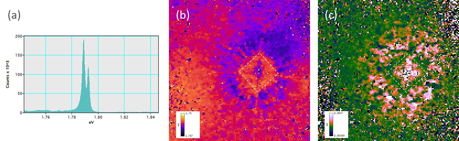
In many wide band gap materials, the wavelength of the luminescence signal is useful to determine stress and strain fields. Luminescence in these materials results from energy transitions involving defects—point defect clusters or impurities—that place an energy level in the forbidden energy gap of the crystal's electronic structure. In many materials, the precise energy of this transition varies as a result of changes in the electronic structure of the crystal under applied stress. Spectrum imaging with high spectral and spatial resolution determines the stress field. The most noted application example of stress mapping is associated with alumina (using the R-line doublet associated with Cr3+); however, other examples include dielectric materials such as SiO2 in semiconductor devices.