Nanostructure Characterization
The size, shape, composition, and structure of nanostructures are known to modify their functional properties, such as their electrical or optical characteristics. The development of novel devices built from nanostructures depends critically on the ability of scientists and engineers to understand the relationship between structure and function. To this end, electron microscopy and luminescence spectroscopy, or photoluminescence (PL),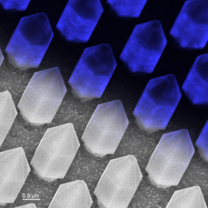 are commonly employed. Electron microscopy helps determine the size, shape, composition, chemistry, and presence of crystal defects of individual nanostructures at or near-atomic resolution. While PL provides insight into band gap and electronic structure. This approach has demonstrated its usefulness with many highly promising devices close to commercialization. However, the PL technique typically measures the average properties of a nanostructure ensemble, and there is a growing realization that the different spatial resolutions used in the two techniques may lead to unsound conclusions.
Cathodoluminescence is a particularly valuable characterization technique for semiconductor nanostructures, providing the power of optical emission spectroscopy at a spatial resolution that enables individual nanostructures to be investigated and, in some cases, individual quantum wells or discs. Furthermore, the availability of other signals in the electron microscope enables a direct correlation of functional properties with sample structure and composition, often simultaneously.