MicroLEDs
MicroLED arrays
Light-emitting diodes (LEDs) are an attractive alternative display technology. LEDs' high emissivity and low power consumption promise significant improvements over existing technologies in augmented reality and mobile device displays. To cover the full-color gamut for displays, LED pixels contain red, blue, and green single LEDs arranged in an array. Hence, the resolution of displays depends on the size and pitch of single LEDs. In efforts to improve resolution by reducing the size of the emitters, the irradiance is consequently reduced. For smaller conventional LEDs to achieve comparable irradiance, they require a higher input power that can lead to more significant heat dissipation requirements.
 |
Cathodoluminescence as a technique for inspection, metrology, and failure analysis of microLED processing |
 Hexagonal core-shell pillar
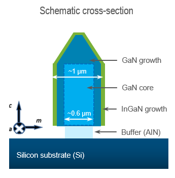
To combat the aforementioned issues that use conventional flat emitters, researchers have turned attention to 3D microLEDs (μLEDs). Such emitters have the apparent advantage of increased surface area, where further the increased dimensionality allows for the formation of quantum wells on the sides of the emitter. The increased dimensionality also provides access to various crystal faces. GaN includes the m-plane, which has a minimal native electric field that reduces the influence of the quantum confined stark effect (QCSE), thereby improving the recombination efficiency of excited carriers.
Compositional variation and defects
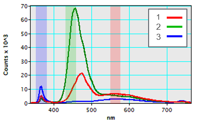
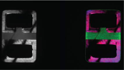
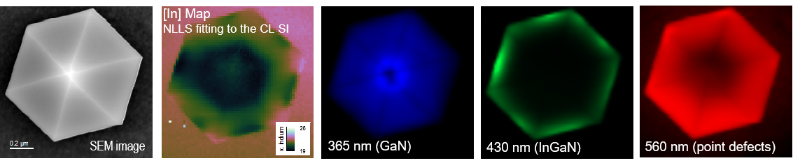
A GaN/InGaN core-shell pillar is a typical 3D emitter. Observing the cathodoluminescence (CL) from such a pillar allows for extracting spectral information as a function of position. Spectral information can be spatially mapped in bands of interest that are readily displayed, e.g., the GaN, InGaN, and point defect bands. Further, in this analysis example, compositional spatial mapping of the InGaN quantum well active layer reveals the In-fraction lies between 19 – 26% and concentrated at the vertices. The native non-linear least squares (NLLS) spectra fitting tool in DigitalMicrograph® software helps estimate the compositional mapping and determine the InGaN band gap as a function of position. The NLLS fitting determined the band gap, which allows for the estimation of In concentration, x, and material composition, which is determined by observing the theoretical band gap of InxGa1-xN as a function of x. Thus far, we have information on spectral CL emissions, but without information concerning the angles of emissions, such shaped specimens can emit anisotropically. To observe such anisotropy, the angle-resolved CL mode of operation can be used.
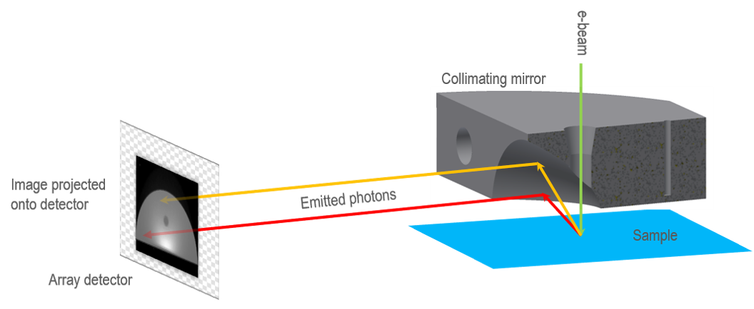
Angle-resolved cathodoluminescence
When light is emitted from a specimen at the focal point of the parabolic mirror, it reflects down the mirror's axis. Mathematically, the paraboloidal shape is 1-to-1. Therefore, the position of the light's reflection on the collimating mirror is unique to the emission angles from the sample. Hence, the angular emission information is acquired by simply imaging the backplane of the paraboloidal collection mirror. With a known mirror shape, you can transform the data into a polar representation for a more straightforward interpretation.
Emission selectivity and shape effects
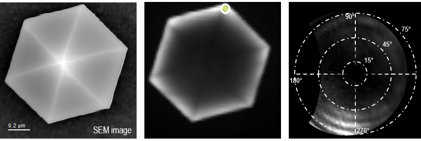
In the case of the single out-of-array microLED pillar, the ARCL revealed an emission selectivity of about 2.4x stronger at ~70˚ compared to the normal direction when integrating the entire pillar. As one might expect, the direction of emission depends on the position of excitation. The emission is most intense in the direction opposite from the side of the pillar, which is excited and includes an interference pattern. The intensity directionality is likely due to the effect of total internal reflection from the index contrast at the pillar surface with vacuum. At the same time, the interference pattern is due to reflections from the sample surface.
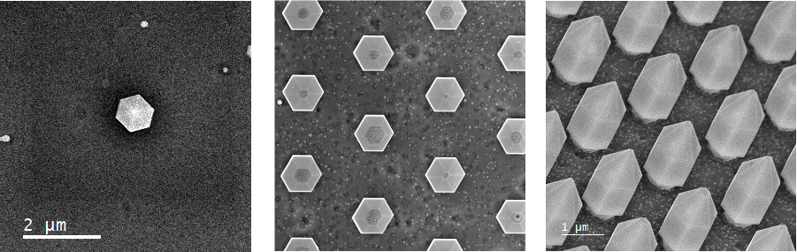
microLED hexagonal pillar array
MicroLEDs are most frequently arranged in an array configuration. In this case, the array configuration is hexagonal with (edge-to-edge) pillar width of ~800 nm and a (nearest neighbor) period of ~2 μm. Such an array using GaN opens the possibility of photonic influences on optical behavior. Therefore, observing them in such an array is essential to determine the impact on light emission.
Effective compositional variation and defects
An in-array single pillar was observed using the same data acquisition as the previously displayed out-of-array pillar. Again, we observe the spectrum for every point scanned in this spectrum image, which allows for emission band mapping of the GaN, InGaN, and point defect bands and estimation of In content by position across the pillar surface. Here, we see an estimate of indium content in InxGa1-xN of between 11 and 19%.
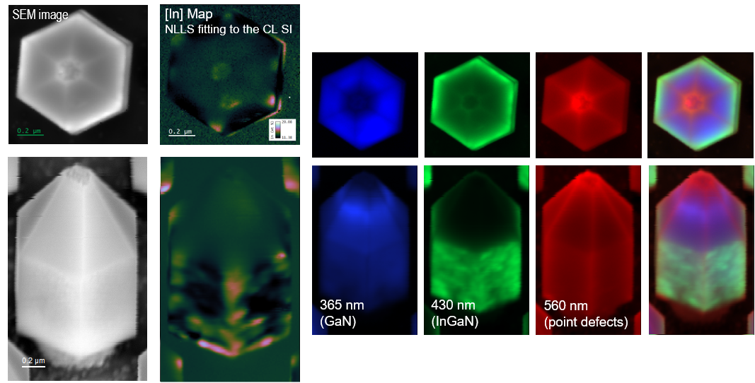
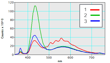
Several interesting observations can be made in this comparison of in- vs. out-of-array microLED pillars. In the out-of-array device, the overall intensity comes from the edge, as expected, since the quantum well is excited directly. Meanwhile, the intensity is more evenly distributed across the surface of the in-array device. Observing spectra from various positions further reveals an enhancement in the overall intensity of the in-array device, especially in the 500 – 600 nm range where multiple smaller peaks are present. The differences are perhaps even more obviated by the color band images of the GaN, InGaN, and point defect bands. In these images, the array influence produces very different emission maps for each excitation position.
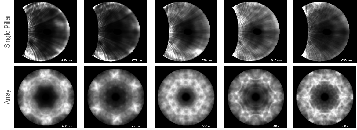
Once the array's influence on light generation is understood, it is common to explore the emission anisotropy as a function of wavelength to determine whether a microLED is feasible for implementation in a display device. To do this, we employ the wavelength- and angle-resolved CL (WARCL) technique, including wavelength information and angular. This reveals any preferential direction of emission and allows for the observation of photonic bandgaps.
Here is a side-by-side comparison of WARCL frames at several wavelengths. The weaker emission in the direction normal to the pillar is present in the out- and in-array LEDs. However, an interesting behavior is present for the in-array, demonstrating the usefulness of the WARCL technique for microLED arrays.
Further information on the photonic crystal behavior of micro-pillar arrays can be found here.