Spatial Mapping
A key benefit of the cathodoluminescence (CL) technique is the ability to capture optical emissions with spatial resolutions (potentially) down to 1 nm—far below the diffraction limit of conventional optical analysis techniques.
You can perform CL mapping in several ways (acquisition modes) to better understand the spatial distribution of materials in your sample and their optical and electronic properties. To acquire this spatial information, a focused electron probe collects CL data (intensity or spectra) on a pixel-by-pixel basis as the electron beam is rastered across the surface of the specimen in a serial manner (X, Y).
There are several ways that the light emitted from a specimen can be analyzed to form a spatially resolved CL map:
- Unfiltered map – Measure the intensity integrated over all wavelengths (and angles and polarizations)
- Wavelength-filtered map – Measure the intensity over a (user-selected) wavelength range
- Color map – Determine the color based on sampling red, green, and blue wavelengths
- Spectrum imaging – Capture the complete spectral information at each pixel
- Angle-resolved spectrum imaging – Obtain the emission pattern at each pixel
At first glance, a CL experiment may seem quite daunting because of the wealth of information generated by the technique. However, the actual workflow is relatively simple:
-
Locate the region of interest within the sample.
-
Set the desired SEM conditions.
-
Ensure the alignment of the CL system to the SEM and sample is correct.
-
Select the field of view (magnification) from which to collect a map.
-
Optimize the map (optional).
This section focuses on capturing a map and optimizing the system to maximize the spatial resolution and signal-to-noise ratio.
Alignment for Mapping
Alignment of the electron beam, cathodoluminescence system, and sample are critical to achieving maps with the highest signal-to-noise ratio and, often, the best spatial resolution. Please refer to the alignment discussion to discover why this is critical and the steps to capture the highest-quality maps.
Collecting Maps
Select the field of view to map
The field of view is determined by the scanning (SEM) magnification setting or scanning transmission electron microscope (STEM). Please consult your microscope manual for details.
Acquire a map
 There are three methods to collect cathodoluminescence (CL) maps: Unfiltered, wavelength-filtered, and color. The appropriate method depends on the type of detector you use. See the modes of operation section for more details.
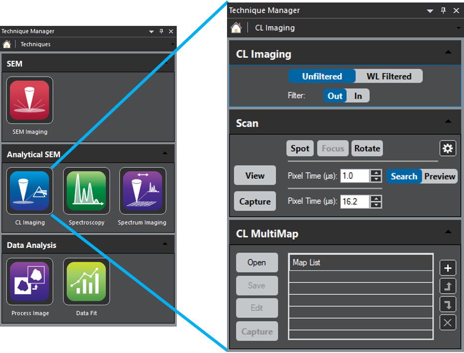
Within DigitalMicrograph® software, go to the CL Imaging or ChromaCL™ technique to collect a map. Regardless of the technique (CL Imaging or ChromaCL), the Scan dialog can collect SEM or STEM images within the DigitalMicrograph software.
- Spot, Focus, Rotate buttons – Control the electron beam: Spot – Sets the beam at a particular location on (or to avoid damage, off of) the specimen, Focus – Scans a sub-region to focus an image.
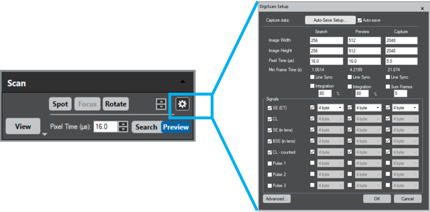
- Setup – Defines the images' pixel time, width, and height (pixels). We recommend capturing at least one signal in addition to the CL signal.
- View – Enables live viewing of SEM or STEM images. When selected, a new image display window opens on the View workspace for each signal you choose within the setup dialog.
- Capture – Records an image using the Capture setting of the DigiScan Setup dialog.
Note: The Scan dialog does not control the type of CL information in a CL map captured by the DigiScan™ system. Instead, the type of detector and acquisition mode you use define the CL information.
ChromaCL color maps
The ChromaCL detector is configured to provide color CL maps. If applicable, simply select the ColorRGB signal alongside the SE and BSE signals in the DigiScan Setup box.
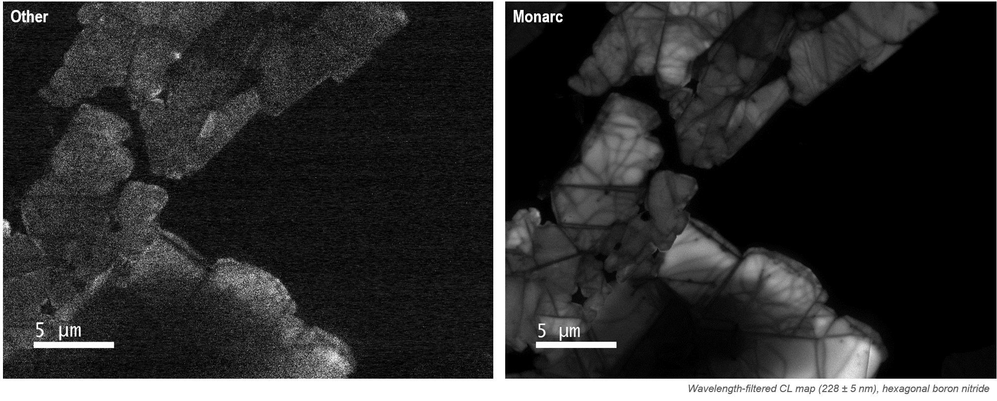
CL maps with Monarc and Vulcan
 Collect a broader range of CL maps with Monarc® and Vulcan® spectroscopic CL detectors. From the CL Imaging palette, configure the spectrograph and detector for the appropriate acquisition mode:
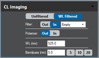
Unfiltered – In this mode, the light bypasses the spectrograph, and the following options are available:
- Filter = In – Selects an optical filter to modify the signal reaching the detector. A drop-down menu allows the user to select one of the five filters installed in the system.
- Polarizer = In or Out – Moves a rotatable polarization filter in or out of the beam path. The user can define the transmitted polarization angle by entering a 0 – 180° range value in the polarization angle text box.
WL Filtered (wavelength-filtered) mode – Focuses photons onto the entrance slit of the spectrograph and disperses them by wavelength (energy). This uses a wavelength-selecting slit to allow a specific range of wavelengths to pass through the system.
- WL (nm) – Sets the wavelength of light that passes through (the center of) the exit slit.
- Bandpass (nm) – Defines the range of wavelengths.
Note that the band pass is the wavelength range that exits the optical spectrograph. For example, when the spectrograph wavelength is set to 525 nm, a band pass of 5 nm corresponds to light in the wavelength range 522.5 – 527.5 nm passing through the spectrograph.
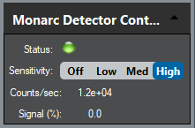 During CL Imaging, a photomultiplier tube (PMT) or diode measures the CL intensity at each pixel. The size of the CL signal can change by many orders of magnitude depending on the sample, SEM settings, and spectrometer state. Use the Detector Control palette to increase or decrease the sensitivity of the CL system.
Note that for PMT detectors, two different DigiScan signals are available: CL Analog and CL Counted. These two DigiScan signals sense the same output from the detector but process the signals differently. The analog signal provides a wider dynamic range, while the counted signal offers a higher signal-to-noise ratio. In many cases, the counted signal is most appropriate, but in the case of very strong emission, the analog signal may be of benefit.
Recipe-driven acquisition of maps (Monarc only)
DigitalMicrograph software allows you to define, recall, and execute a sequence of maps using the MultiMap palette. When the + icon is selected, the software stores the current DigiScan, spectrograph, and detector settings and then defines a sequence of maps. The user may name these steps to their liking and save a recipe for recall later.
Optimizing Maps
Collecting the highest-quality maps depends on many factors, including the sample, microscope setup, and system alignment. Read below for more information.
Scanning electron microscope (SEM)
Many mechanisms generate the cathodoluminescence (CL) signal in an SEM. The following section describes optimizing the SEM and CL hardware to capture CL data with the highest spatial, spectral, and angular resolutions.
Absorption of an electron's energy: Electron-sample interactions
When the electrons (of the electron microscope's electron beam) strike the sample, they interact with the crystal, transferring some of their energy to the sample. Each interaction only transfers a small fraction of the electron's energy. Consequently, each electron undergoes many interactions as it travels through the crystal before losing all its energy or exiting the specimen.
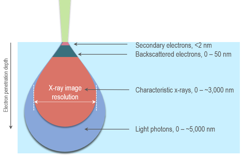
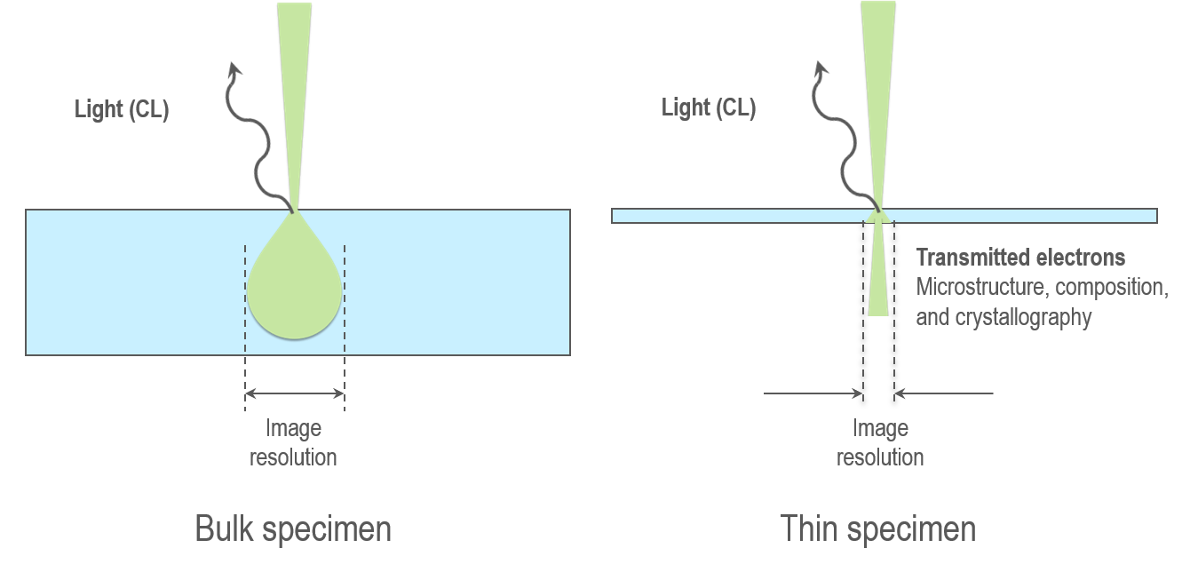
SEM imaging analyzes the crystal region where electron-sample interactions occur, known as the interaction or generation volume. As the electrons penetrate below the surface, they undergo scattering events that cause them to spread laterally. Thus, the interaction volume is typically described as pear-shaped, as shown pictorially here.
Within the interaction volume, electron-sample interactions give rise to electron or photon signals that may be useful for image formation or spectroscopic analysis in the SEM. To detect these signals, the electron or photon must exit the sample. However, some electrons and photons do not escape and may be re-absorbed by the sample crystal. Electron signals typically originate within a few –or few tens of– nanometers of the sample surface, whereas photons (e.g., x-rays or cathodoluminescence/light) can escape from several micrometers below the surface. A consequence is that an SEM image's spatial resolution depends on the lateral extent of the interaction volume for a given signal. The greater lateral extent of the interaction volume results in a lower image resolution for signals generated deep within the specimen.
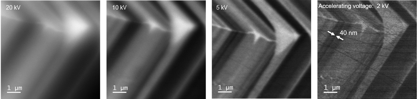
For photon signals, the lateral extent of the interaction volume depends greatly on the SEM's accelerating voltage. Here, we show CL images captured from the same region of a polished zircon mineral at three different accelerating voltages. The spatial resolution improves as you reduce the accelerating voltage due to the smaller lateral extent of the interaction volume. In all three cases, the electron beam was focused on a spot smaller than 1 nm in diameter, and no difference in the secondary electron image resolution was observed.
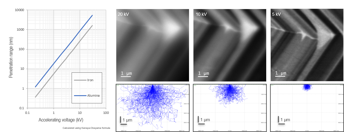
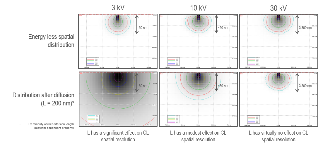
You can mathematically model the size of the interaction volume using a Monte Carlo simulator, such as CASINO. A comparison of the interaction volume for zircon at the three analysis conditions is shown. However, note that the precise size and shape of the interaction volume depends on the microscope settings and the sample analyzed. Nevertheless, such modeling is relatively simple to perform, can predict the achievable image resolution, and can be useful to optimize the SEM settings for a given sample. It's also important to note that the penetration depth of electrons decreases with the accelerating voltage. This must be considered when analyzing sub-surface features (e.g., buried quantum well structures in semiconductor specimens). But more importantly, it provides an opportunity to gather depth-resolved CL information (e.g., differentiating between surface and bulk effects).
The energy of the electron beam is often continually variable in modern SEMs. One temptation is to use the smallest accelerating voltage possible; however, there are some limitations and consequences to that:
- The incident electron's energy must be large enough to generate the signal still.
Many characteristic x-rays have an energy of 5,000 – 10,000 eV, thus requiring accelerating voltages greater than 5 – 10 kV, respectively. CL photons have energies lower than 6 eV and may be generated in most SEM settings.
- As you reduce the electron beam energy, it generates fewer photons per electron.
The incident electron's lower energy results in fewer interactions with the host crystal before its energy is lost, generating fewer photons.
- Surface effects become more pronounced.
When the interaction volume is closer to the sample surface, the surface plays an increasingly important role when you reduce the accelerating voltage. In many samples, the surface reduces the photon emission rate due to an increased prevalence of defects that result from sample preparation and dangling bonds.
These effects can be seen in the CL image of the zircon captured at 2 kV. Here, the interaction volume extends only 20 – 30 nm below the surface of the specimen. High spatial resolution is observed, with features narrower than 40 nm resolved. However, you can see an overall reduction in the image signal-to-noise and dark lines from scratches introduced during mechanical polishing.
In many cases, the reduction in the signal at low accelerating voltages places a practical limit to the best achievable spatial resolution. Thus, the sensitivity of the CL system is a key concern when trying to achieve the highest resolution results.
Transformation of energy: Internal processes within a sample
When a solid absorbs energy from the incident electron beam, several physical processes may occur shortly before a photon is released to return to the energy ground state. In semiconductors, one must consider the effect of minority carrier migration by drift and diffusion, and in metals, the propagation of surface plasmon polaritons.
First, you must consider the impact of the minority carrier diffusion processes in semiconductors.
- The electron beam generates an excess of free carriers (electron-hole pairs)
- The top 3 images show the extent of the interaction volume at three different accelerating voltages; this is a snapshot of the electron-hole pair distribution before diffusion
- The excited carriers are free to move in response to local electric fields (drift) or diffuse according to the minority carrier concentration gradient
- How far the free carriers move is determined by the minority carrier diffusion length—a measure of how far free carriers move on average before they recombine—which is a material-specific parameter
- In a homogeneous material, the minority carrier diffusion length can be larger than the extent of the interaction volume and become the limiting factor for spatial resolution in the CL map
- For a given material, there is a limit to the spatial resolution that may be achieved driven by the material's property rather than the accelerating voltage employed by the SEM
However, most semiconductor materials of interest are not homogeneous; they contain defects such as grain boundaries, stacking faults, and dislocations that modify the local recombination behavior. One consequence is that it is possible to resolve features of interest smaller than the minority carrier diffusion length in CL maps.
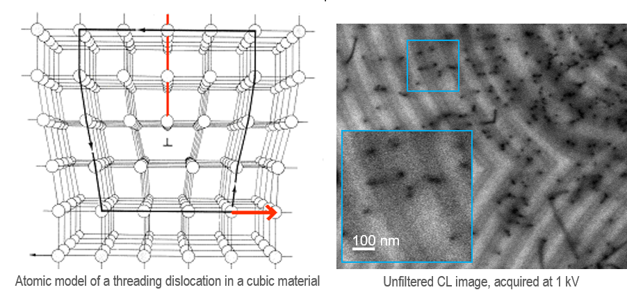
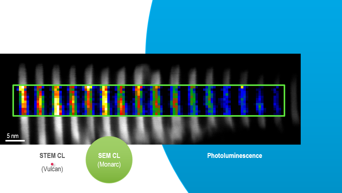
CL mapping is commonly employed to quantify the electrically active dislocations in gallium nitride (GaN). GaN is a base material for LEDs and high-power transistors but contains a high dislocation density that can reduce device efficiency and increase leakage current. Many device manufacturers believe it is important to quantify the dislocation density since they act as non-radiative recombination centers. In the example above, the black spots correspond to the individual (1D) threading dislocations, which are viewed end-on, given the sample geometry. CL measurements show the threading dislocations are ~50 nm in diameter, larger than the interaction volume (<20 nm) but smaller than the minority carrier diffusion length of 100 – 150 nm.
Emission of excess energy: Photon generated as sample relaxes to the ground state or photon escapes into vacuum space
Photons are generated within a material. However, to detect the photon, it must escape from the specimen.
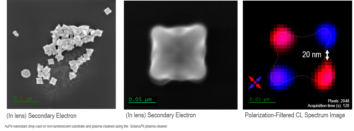
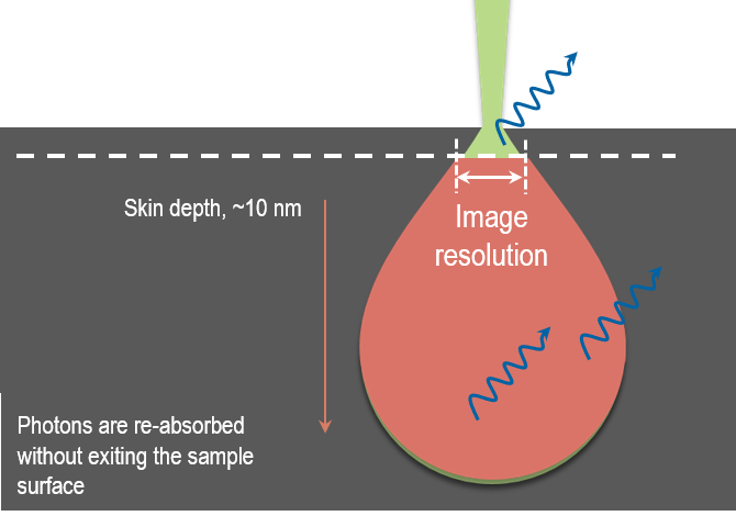 In transparent samples, the photons must pass through the sample and across the sample-vacuum interface to be detected. However, this is not the case for all samples. The photons may be re-absorbed in semi-transparent or opaque materials before they can escape. In the case of metals, this escape depth is limited to the material's skin depth (a property of the material). Thus, the image resolution is no longer limited by the size of the interaction volume but rather by the lateral spread of the interaction volume at the skin depth of the material. A CL map can achieve a spatial resolution of 10 nm in many metals and is independent of the SEM's accelerating voltage.
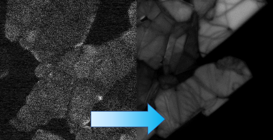
The below results show an AuPd nanostar analyzed at 20 kV accelerating voltage. The lateral spread of the interaction volume is 1 µm (larger than the particle itself); however, a spatial resolution in the polarization-filtered CL spectrum image is clearly better than 20 nm.
SEM alignment
Optical alignment is a key concern in mirror-based systems, as incorrect alignment can waste more than 99.99% of the photons.
 One consequence of employing a collection mirror is that the alignment of the sample, the e-beam of the scanning SEM, and the CL system become very important. Consider the simplified schematic of a CL detector shown.
You can assume that light emerges from the sample at the point where the electron beam is located. If the sample and CL system are aligned well, the light reflects from the collection mirror in a collimated ray bundle as light rays travel in parallel. Often, transfer optics like lenses, mirrors, or optical fibers are employed to transform the ray bundle to match the shape of the photon-sensitive area of a detector (e.g., a photomultiplier tube or a solid-state diode).
The detector provides a signal whose magnitude depends on the photons' detection rate, typically described as the (detected) CL intensity in units of counts/s. However, the electron beam can be scanned across the sample surface in a defined pattern, and the CL intensity is measured at each pixel. This forms a CL Map (2D data) that describes the spatial variation of the photon emission rate from the sample and may be unfiltered (contains no wavelength information) or a wavelength-filtered CL map (allows a limited range of wavelengths to reach the detector and contribute to the measured signal).
If the electron beam moves outside the CL system's focal range, the light no longer travels through the optical system in an intended manner, and few photons reach the detector. This photon loss results in a variation in the brightness of a CL image purely based on the non-uniformity of the light detection at low magnifications. This can be observed in the SEM at magnifications below ~200x, where the CL Map reveals a bright region—sometimes referred to as the sweet spot or hot spot. To maximize sensitivity and faithfully interpret CL Maps, aligning the sweet spot to coincide with the center of the SEM beam's scan pattern is critical. In other words, as the magnification of the SEM increases, the field of view of the CL map remains within the sweet spot.
To achieve this, the specimen must be precisely located at the focal point of the collecting objective, and the optical axes of CL and SEM systems must be co-aligned within a few microns.
To do this:
-
Align the sample with the CL system (z) by finding the sweet spot.
-
Align the CL system (x,y) to the e-beam axis of SEM (x,y) by repositioning the sweet spot to appear at the center of the field of view.
-
Focus e-beam at sample region of interest (z).
For more details, refer to the alignment section in Getting Ready
Transmission electron microscope (TEM)
In the TEM CL setup, a thin specimen greatly simplifies the collection of high-resolution maps. In thin specimens, the lateral spread of the interaction volume is typically less than one or two nanometres, even for relatively thick specimens.
However, you must consider the minority carrier diffusion and transport of surface plasmon polaritons. In heterogeneous materials, you can achieve a spatial resolution approaching 1 nm.