Plasmonics
Plasmons are a collective oscillation of electrons in a material caused by the co-mingling of electric and magnetic fields. Plasmonics can refer to shapes, materials, and interfaces that exhibit behaviors like plasmon propagation (polariton) or resonance. Plasmons can occur in a volume or at a surface, known as a surface plasmon (SP), and can have an effective wavelength much shorter than their free-space counterparts.
The interaction of light causes the resonance of the free electrons. This leads to greatly enhanced electromagnetic fields, particularly in noble metal structures, which can be used in waveguides to enhance light or particle detection and catalysis. Plasmonic metal-based nanoparticles attract significant attention due to numerous novel optical device designs that utilize a nanostructure's size, shape, and composition to enhance light emission and absorption. With qualities such as durability, high spatial resolution, and tunable viewing angle, plasmonics offer significant potential for optical elements in high-resolution color printing and high-density data storage. Recent advancements in nanofabrication technology offer fabrication simplicity with control over the shapes of nanoparticles.
The identification of the plasmon resonance modes and hot spot locations is critical. Still, it presents a significant experimental challenge due to weak light emission levels and smaller particle size than the diffraction limit.
Cathodoluminescence (CL) is a natural technique for plasmonic investigations for myriad reasons. Plasmons can be stimulated through interaction with photons (as in a photoluminescence (PL) experiment) or energetic electrons of an electron microscope. The electron beam probe size used in CL microscopy is on the order of a few nanometers, thus providing much higher spatial resolution than PL and generating other signals to determine sample size, shape, structure, and composition. Furthermore, the energetic electron probe can be considered a broadband excitation source whereby the plasmonic modes excited do not rely on the wavelength (energy), direction, or polarization specificity of the excitation source. CL output data would not contain influence from the excitation source as it may in a PL experiment.
Results from an Au-Pd nanostar deposited on a (non-luminescent) silicon substrate are shown as an example. Secondary electron imaging (a) revealed the nanostar to be approximately 100 nm on edge, and CL spectrum imaging revealed intense emission (wavelength of 600 nm) emitted when the electron beam was positioned at the nanostar tips, indicative of plasmonic resonance between the nanostar tips. Polarization-filtered spectrum imaging revealed the resonance as dipolar modes from opposing tips (red and blue in (b)).
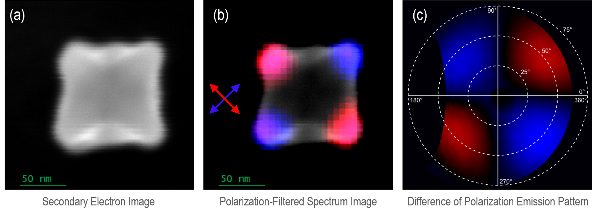
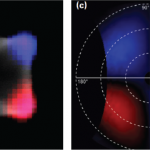
Angle-resolved CL (ARCL) emission patterns were recorded from each tip of the nanostar (e.g., each resonance node). The difference in emission patterns from each resonance mode is displayed in (c), highlighting distinct emission patterns associated with each mode.
Experimental briefs and application notes
 |
 |
| Determining photonic band structure by energy-momentum spectroscopy in an electron microscope | Investigating the optical properties of nanophotonic materials far below the diffraction limit |