Cathodoluminescence (CL) emission helps explore many properties of a sample, finding use in applications ranging from fundamental research to industrial metrology and failure analysis. Many other techniques cannot access this information-rich data. However, the attainable information can be very sample-specific:
Geoscience: Cathodoluminescence microscopy reveals the real structure of solids based on a crystal's intrinsic properties and trace-element chemistry. CL is frequently used to reveal the process(es) of formation and alteration to reconstruct geological processes in minerals. Although beneficial for identifying minerals (and their distribution), this may be achieved more easily using energy-dispersive x-ray spectroscopy (EDS or EDX).
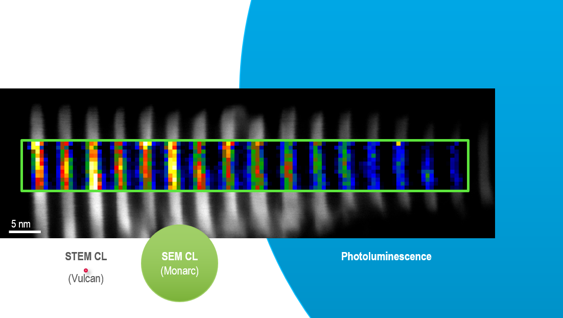
Materials science: Spectroscopic CL microscopy enables the study of a semiconductor material's electronic structure, e.g., measuring bandgaps and revealing crystal defects. For these reasons, CL characterization is important in optoelectronic materials and device development, including the laser, photovoltaic, light-emitting diode (LED), and microLED display industries. In nanophotonics, CL light-emission maps reveal the local density of electromagnetic states and determine the directionality and polarization of emission, providing detailed insight into nanostructure optical properties.
Benefits
CL analysis in an electron microscope provides several unique benefits over other luminescence techniques, including:
-
Optical information down to the nanometer-scale spatial resolution
-
Direct correlation with structure, chemistry, and crystallography
-
Analysis of optically transparent samples
Optical information with nanometer-scale resolution
The spatial resolution of conventional optical microscopy—and its associated luminescence imaging and spectroscopy techniques—is limited due to Abbe's law of diffraction. Abbe's law of diffraction states that, in a perfect optical system, it is impossible to resolve two points that are spaced less than half of the wavelength of the light source. For an ideal microscope using a blue laser (wavelength 400 nm), spatial resolution is no better than 200 nm, thus making conventional optical microscopy unsuited for studies at the nanoscale.
On the other hand, the wavelength of electrons in an electron microscope is <1 Å, which allows you to resolve information at the nanoscale. The precise spatial resolution of CL microscopy depends on several factors, including the sample type and structure. However, studies demonstrate spatial resolutions approaching 1 nm, a length relevant for many optical devices based on optoelectronic or nanophotonic materials.
Correlation with structure, chemistry, and crystallography
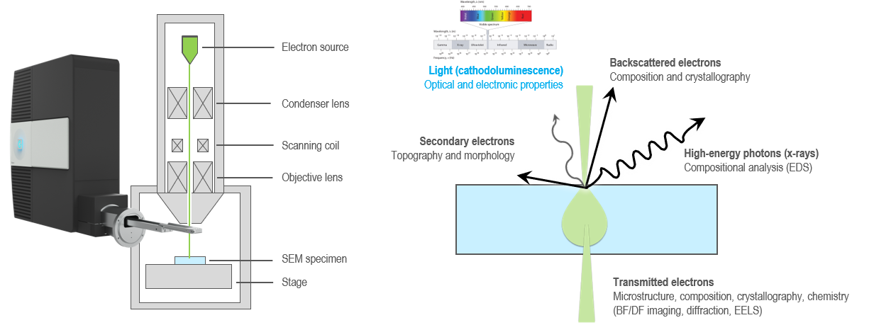
When an electron beam interacts with a material, a multitude of processes occur that are employed for various kinds of microscopy and microanalysis. You can analyze the size, shape, topography, composition, crystallography, and chemistry of a sample using the various electron and photon signals that are emitted. This enables you to correlate nanoscale geometrical features with the optical response that a CL detector records.
Analysis of optically transparent samples
Electrons interact with matter far more strongly than photons. Thus, the energetic electrons of an electron microscope are helpful as an optical excitation source for transparent materials, acting as a probe-less and (mostly) nondestructive broadband excitation source. This makes CL particularly useful for characterizing wide band gap semiconductors and insulators, such as many engineering ceramics, rocks, minerals, and gems. In insulator materials, CL photons largely originate from impurities or crystal defects. This makes the CL technique particularly useful for trace element microanalysis in geological samples.
Experiment briefs and application notes
 |