Stress mapping in engineering ceramics
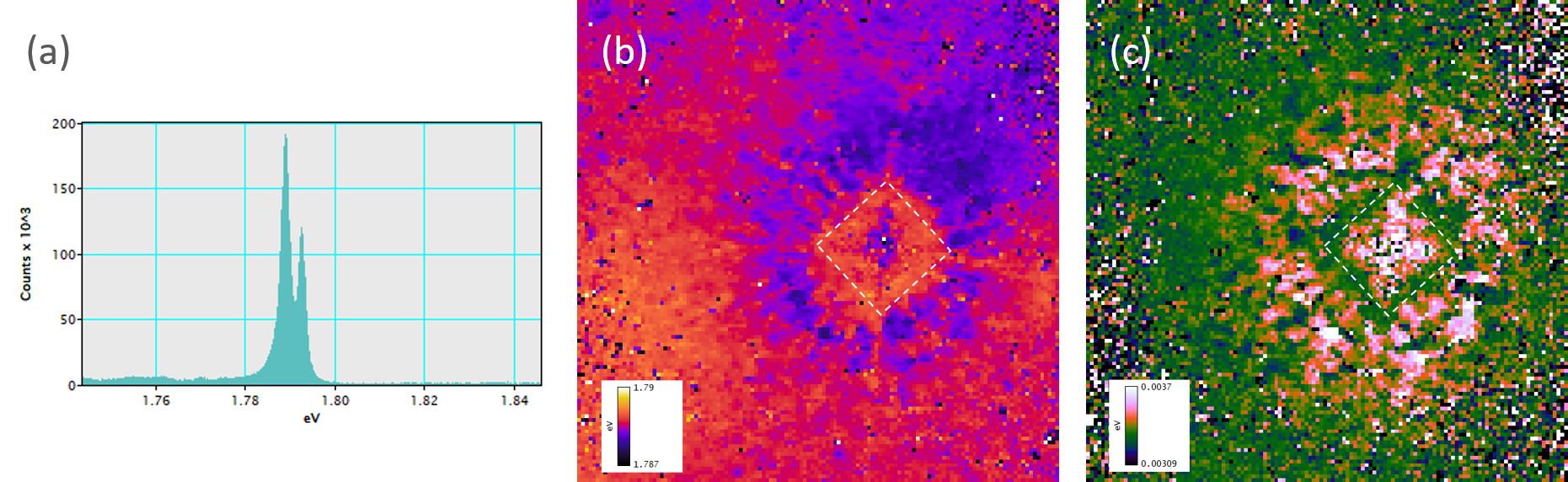
In many wide band gap materials, the wavelength of the luminescence signal is useful to determine stress and strain fields. Luminescence in these materials results from energy transitions involving defects—point defect clusters or impurities—that place an energy level in the forbidden energy gap of the crystal's electronic structure. In many materials, the precise energy of this transition varies as a result of changes in the electronic structure of the crystal under applied stress. Spectrum imaging with high spectral and spatial resolution determines the stress field. The most noted application example of stress mapping is associated with alumina (using the R-line doublet associated with Cr3+); however, other examples include dielectric materials such as SiO2 in semiconductor devices.