Cathodoluminescence (CL) maps often provide distinctly different information from other signals in the electron microscope. Many other signals are formed due to directly observable physical features such as sample size, shape, and topography. However, the information gathered from the CL signal is related to the local optical and electronic properties, and the correct interpretation often requires careful consideration.
Insulators Semiconductors Metals
You can separate solid materials into three distinct groups based on their electronic structure: Metals, semiconductors, and insulators. Every solid has its characteristic energy-band structure, and the variation in band structure is responsible for the wide range of electrical and optical characteristics observed. In a CL experiment, the luminescence that we measure is a direct result of the interaction of the high energy electron of our electron beam and the sample's electronic structure. Thus, measurements are sensitive to changes in the electronic structure, including a change in the energy of the crystal’s band gap (composition, stress, temperature) and electronic levels within the band gap (e.g., intentional or unintentional doping/impurities, crystal defects, charge state).
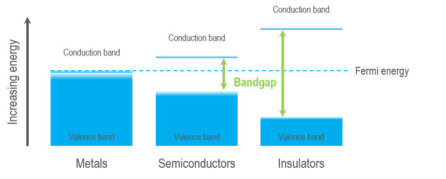
Semiconductors and insulators are characterized by a band gap—the (energy) distance between the valence band of electrons (electrons bound to an atom or ion in the crystal) and the conduction band (where electrons are free to move within the crystal). The band gap is a range of energy states that an electron is forbidden to occupy, and energy equal to or greater than the band gap energy must be provided to excite a valence electron into the conduction band. A semiconductor is a material with an intermediate-sized band gap, whereas a material with a large band gap is an insulator. The valence and conduction bands overlap in conductors, and electrons are free to wander the crystal, enabling metals to conduct electricity efficiently.
Insulators
Let us first examine the case of CL from insulators such as rocks, minerals, gems, and other dielectric materials. The electron beam imparts energy to the crystal of the sample and can promote an electron from the valence band to the conduction band. However, this energetic state is unstable, and the crystal returns to the ground state by the electron falling from the conduction band to the valence band. The excess energy transforms into heat (phonons)and light (photons), with the photon's energy release corresponding to the energy transition's size.
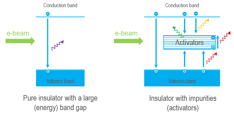
Nevertheless, the energy gap of insulators is too large to produce photons at visible wavelengths (\(Energy ∝ 1/Wavelength\)). Instead, CL at visible, ultraviolet, and infrared wavelengths (180 – 2300 nm) is produced via activators—transition metal ions, rare earth ions, or crystal defects—which place energy levels within the band gap. The emitted photon's energy (wavelength/color)relates to the energy transition(s) and activator species in a crystal. CL mapping and spectroscopy can reveal the presence and distribution of activators and identify the activator species, making them powerful tools for the microanalysis of geological minerals.

Here is an example of a color CL map. The map differentiates minerals and reveals the distribution of trace elements within individual grains at concentrations as low as 1 – 10 parts per million, making CL an effective tool for reconstructing geological processes based on crystal chemistry. For more information on using CL maps for microanalysis, please refer to the Rocks, Minerals, and Gems section.
Semiconductors
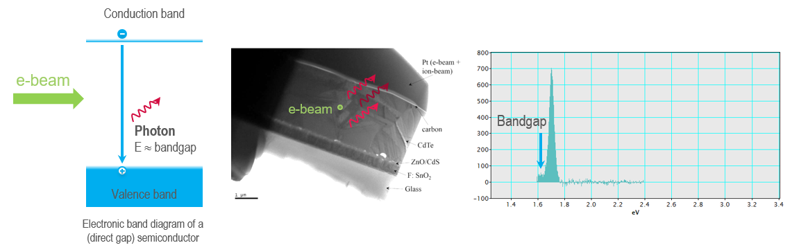
Its electronic structure and band gap govern a semiconductor's useful properties. Scientists and engineers strive to understand and control these properties to create more efficient devices or devices with novel properties like transistors, lasers, light-emitting diodes, and solar cells. Semiconductor materials have a narrower band gap than insulators (0.5 – 6.0 eV typically), and in these materials, the relaxation of an electron from the conduction band to the valence band (termed band-to-band recombination) often emits a photon with a wavelength that may be termed cathodoluminescence. Thus, CL can be used to determine the band gap of material (often) with nanoscale spatial resolution. In the example below, a CL spectrum reveals the band gap of a CdTeS solar cell, enabling the alloy composition to be mapped with high precision.
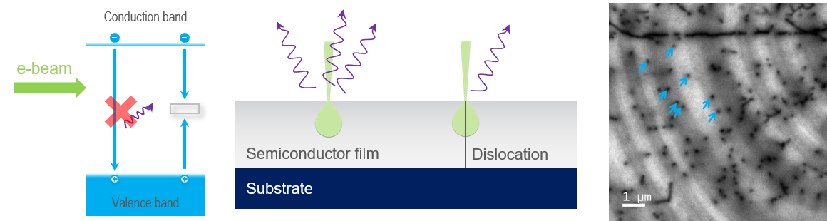
In semiconductors, many crystal defects introduce deep levels into the band gap. Unlike activators in insulators, energy transitions that take place via deep levels do not release a photon. The band-to-band and deep-level recombination pathways are competitive; thus, when a semiconductor crystal contains defects (that introduce a deep level), the probability of photon emission is reduced and, in a CL map, can be revealed as areas of dark contrast. In the example shown here, threading dislocations in a semiconductor film are observed where they intersect the surface of a GaN film.
Revealing the electronic structure of defects at cryogenic temperatures
Non-radiative recombination via deep levels requires phonon participation. The phonon population can be reduced at cryogenic temperatures so that radiative recombination via the defect levels becomes probable. Cryogenic SEM stages are often used with CL detectors to allow the electronic structure of crystal defects to be determined.
Metals
Metals do not have an electronic bandgap yet can still emit light in a CL experiment; however, the mechanism for light emission is quite different from that of semiconductors and insulators discussed previously.
Metals are characterized by having free electrons in the conduction band. These free electrons govern their optical and electronic properties; the sea of free electrons moves through the crystal in response to an electric field to conduct electricity and also controls their optical properties. The electric field of visible light oscillates extremely rapidly and can cause the free electrons near the metal's surface to oscillate in response. Under the right conditions, the light wave can excite a longitudinal wave of electrons known as a surface plasmon. Not all metals can support surface plasmons, and typically, they exist only over a narrow frequency (wavelength) range; however, the surface plasmon has some potentially fascinating advantages:
- Field enhancement—The electric field is extremely localized, which results in plasmonic field amplitudes that can be two orders of magnitude larger than the electric field that excited the plasmon; the plasmonic metal behaves like an antenna.
- Long-range propagation—Typically, light does not penetrate very far into a metal (only a few nanometers). However, surface plasmons can travel up to a millimeter along a metal's surface, opening the possibility for integrated optical and electronic circuits.
- Short wavelength—A surface plasmon has a shorter wavelength than the light of the same frequency does, implying that surface plasmons can be used to focus light below Abbe's optical diffraction limit.
There has been much interest in metallic nanostructures as the surface plasmons may be controlled by a nanostructure's size, shape, and composition. In particles smaller than the propagation length of the surface plasmon, surface plasmon resonances may be established with control over the resonant frequencies, providing a toolbox for developers of nanophotonics devices. Revealing plasmon resonance modes is critical but presents a significant experimental challenge given the sub-diffraction limit particle size and low luminosity.
Energetic electrons can also generate surface plasmons, and in the electron microscope, we can use CL to analyze surface plasmon behavior, as light absorption and emission are reciprocal processes. Furthermore, we can directly correlate the physical structure to the optical properties.
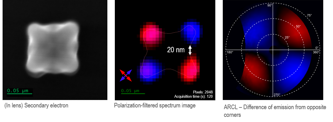
The figure below shows an individual AuPd nanostar, ~100 nm tip-to-tip. The CL map reveals four bright spots, each located at the tip of an arm of the nanostar with strong emission at a wavelength of 600 nm. These hot spots in the CL image correspond to maxima in the local density of optical states in the nanoparticle occurring at the resonance nodes at the nanostar tips. The differing emission polarization at the nodes suggests that the most intense plasmonic modes are dipolar and resonant at opposing tips.
The ability to interrogate the interaction of light and matter far below the diffraction limit with wavelength (energy), polarization, and angle (momentum) resolution makes CL an ideal technique for nanophotonics studies. For more information, please refer to the Nanophotonics section.