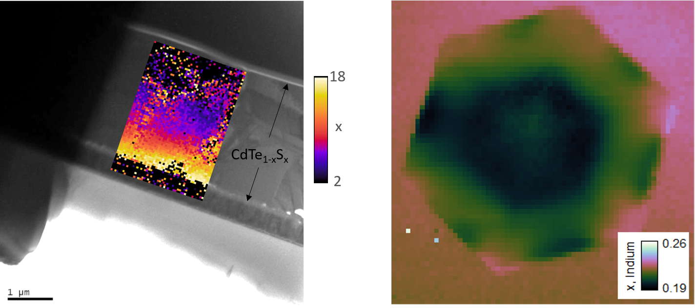
Composition and doping metrology
For many devices, optimized performance relies on careful control of the alloy composition of compound semiconductor crystals, epitaxial layers, or nanostructures. Whether that is producing homogeneous layers with a composition that is very close to the target value in the manufacture of GaAs solar cells, nitride-semiconductor quantum wells for light-emitting diodes, or the through-thickness graded alloy of a CIGS thin-film solar cell; cathodoluminescence (CL) proves to be a superior technique offering rapid, non-contact, analysis that also benefits from nanoscale spatial resolution.
Experiment briefs and application notes
Defect detection and characterization
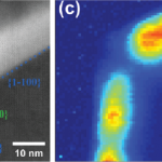
CL microscopy is helpful in revealing the presence and distribution of subsurface crystal defects, such as dislocations and stacking faults, in semiconductor wafers and epitaxial layers. During a measurement, the CL signal shows the local recombination activity of electron-hole pairs and excitons. Additionally, as recombining electron-hole pairs is a competitive process, it reveals non-radiative recombination at electrically active defects as dark contrast in a CL map (see below).
Understanding the electronic structure of crystal defects can prove vital when devising methods to nullify the deleterious effect on device performance. Spectroscopic CL is one of the few methods available to provide a detailed understanding of the distribution, concentration, and energy levels of deep-level states associated with crystal defects. At cryogenic temperatures, non-radiative recombination becomes less probable due to the reduced phonon population, making possible radiative transitions via the defect states. Therefore, spectrally resolved CL can be used to determine the mid-bandgap energy level(s) of defects from the radiative emissions, and the spatial resolution of CL enables measurement of the distribution and concentration of defects.
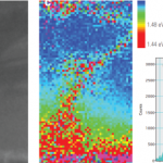
Lifetime and/or minority carrier diffusion
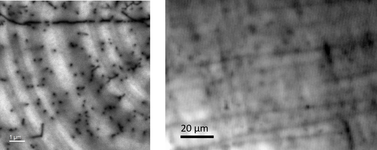
In a semiconductor, the electron beam of the electron microscope generates free electrons and holes. Before recombination, the excess carriers can move within a crystal under drift and/or diffusion mechanisms. Under most experimental conditions, the concentration of these free carriers is far below the majority carrier density concentration of a doped semiconductor, so we typically only need to consider the behavior of the excess minority carriers (or excitons). CL maps may capture this effect so you can observe when the generation volume is small (e.g., at low accelerating voltages): In the CL map of a GaN wafer containing threading dislocations (above), the black dots correspond to an individual threading dislocation intersecting the surface. These defects are one-dimensional, yet the dark spot in the CL map has a diameter >50 nm. This demonstrates that the dislocation impacts the crystal's electrical properties over a more extended range than the dislocation's physical extent or a fraction of the free carriers generated within the minority carrier diffusion length diffuse to the dislocation and recombine non-radiatively. Empirical models are available to extract the minority carrier diffusion length from CL maps of crystal defects. However, recent research demonstrates that time-resolved or spectrally resolved measurements at cryogenic temperatures are superior.