A semiconductor is a generic term for materials with electrical conductivity between conductors (copper and aluminum) and insulators (rubber and glass). There are few elemental semiconductors, but there are widespread commercial applications in microelectronics and photovoltaics. However, other elements may be combined to form compound semiconductors—alloys with properties of a semiconductor, e.g., GaAs, GaN, CdTe, and (many) others. Despite the high cost of manufacture, compound semiconductors form the basis of many modern devices, including light-emitting diodes, power transistors, and detectors, because of their attractive fundamental material properties, including efficient light emission across the ultraviolet, visible, and infrared portions of the electromagnetic spectrum.
The light emission from semiconductors can be used to reveal the functional properties of the material that directly impact the performance of many commercial devices. The ability of the cathodoluminescence (CL) technique to analyze the light emission at a spatial resolution commensurate with the device feature size and to correlate that information with the composition, size, shape, and crystal structure makes CL a highly valuable technique. For example, the functional properties of compound semiconductor materials and devices depend critically on the sample structure, compositional uniformity, and defect concentrations and distribution, all of which can be revealed in detail using CL. For these reasons, CL is used widely in process development or material and device characterization.
-
-
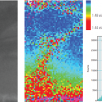
Composition and doping metrology
-
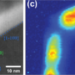
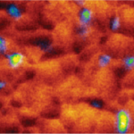
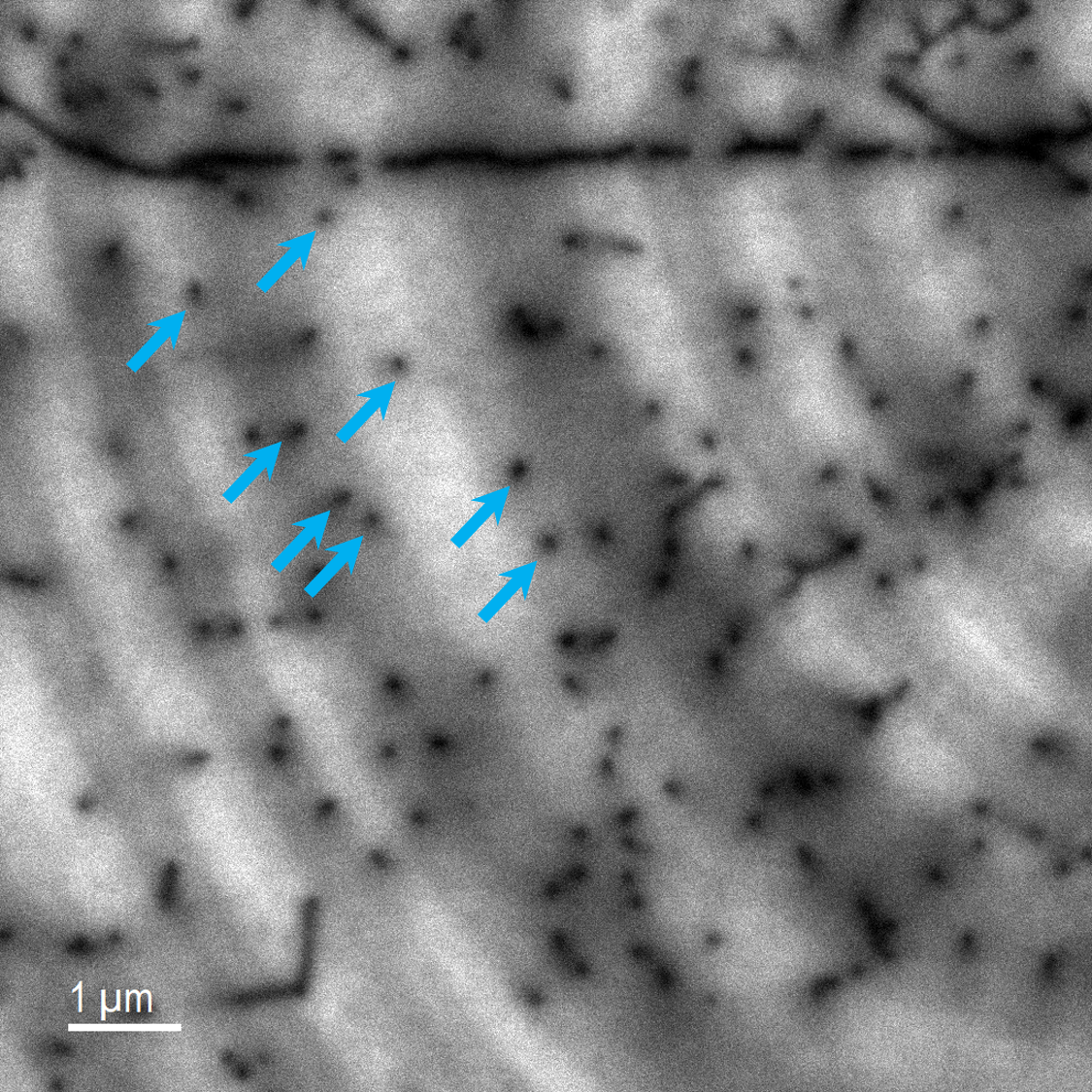
Defect detection and characterization
-
Lifetime and/or minority carrier diffusion
-
-
-
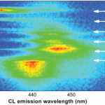
Light-emitting diodes and microLED arrays
-
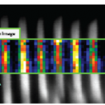
Aging studies and failure analysis of laser diodes
-
Photovoltaics
-