Light-emitting diodes (LEDs) are more efficient, faster, and have a much smaller footprint than filament-based light sources. LEDs are composed of semiconductor materials whose electronic density of states includes a forbidden band known as the band gap. When electrons and holes are excited and allowed to recombine across the band gap in a semiconductor, the emitted photon (observed as light) carries the energy of the band gap. The advent of the blue LED in the 1990s and the subsequently explored tunability of the III-nitride materials paved the way for LED-based lighting and display technologies.
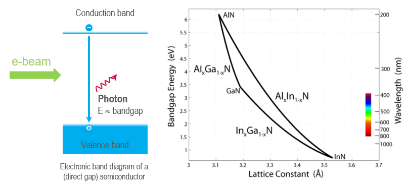
For LED applications, GaN is usually grown in a heterostructure form with a number of InxGa1-xN quantum wells (QWs). These generate efficient light emission in the visible part of the electromagnetic spectrum rather than at the native (GaN) band gap energy of 3.4 eV (365 nm). They are useful for enhancing gain and optical confinement by increasing the active region volume and allowing the tunability of the emission color (wavelength).
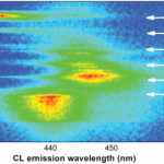
The cathodoluminescence (CL) technique is a fast and highly relevant method in the process development of GaN LEDs. The energetic electron beam can effectively excite the wide band gap of nitride semiconductors (even AlN) and provide spatial resolution down to 10 and 1 nm for CL measurements performed in the scanning electron microscope (SEM) and transmission electron microscope (TEM) instruments, respectively. One can directly visualize the distribution of non-radiative defects, such as dislocations, and determine the identity of point defects. Furthermore, the spatial variation of strain, doping, growth direction, and carrier concentration can all be determined, as well as the different constituents of the stack (e.g., AlN, GaNs, quantum wells).
In addition, you can visualize the emission pattern using the angle-resolved or wavelength- and angle-resolved modes of operation. These modes offer another significant metric for light-emitting devices as they enable detailed spectra characterization using angle-resolved CL imaging.
Experiment briefs and application notes
 |
 |
| Cathodoluminescence as a technique for inspection, metrology, and failure analysis of microLED processing | Nano-cathodoluminescence enables the design of light-emitting diodes with higher efficiencies |
3D metrology of an LED structure
While CL provides high-lateral spatial resolution to investigate semiconductor materials, it also enables depth-resolved measurements. Using the selected accelerating voltage of the SEM to determine the surface depth that the CL signal is generated from enables the analysis of layers buried within the bulk material. Furthermore, it allows the investigation of 3D structures by depth-resolved CL spectroscopy, which compares the simulation of primary electron scattering with carrier drift and/or diffusion. Such depth-resolved measurements enable:
- Mapping of the depth and lateral distribution of dislocations and basal plane stacking faults in fully processed devices
- Thickness measurements of sub-surface layers of different compositions, including analysis of individual quantum wells within a multi-quantum well stack
- Location of point defects at specific interfaces within a device structure (with ~1 nm axial resolution)
Failure analysis
General lighting applications and car lights frequently use white and blue LEDs, but their use also penetrates more diverse purposes, including industrial environments. In such environments, the devices are subject to extreme environmental conditions such as mechanical vibrations, or enhanced or extremely low temperatures, humidity, or chemical substances. There is a growing realization that the LED chip itself, rather than a peripheral element, can lead to module failure under these conditions. With such a diverse range of applications, laboratory testing procedures can't replicate all use cases in real field applications. It is, therefore, necessary to use analytical techniques capable of observing the LED structure on a macroscopic and microscopic scale, characterizing both physical structure and functional properties. To this end, electron microscopy, including CL, is an attractive and effective tool in evaluating failure causes in light-emitting devices.