Semiconductors
A semiconductor is a generic term for materials with electrical conductivity between conductors (copper and aluminum) and insulators (rubber and glass). There are few elemental semiconductors, but there are widespread commercial applications in microelectronics and photovoltaics. However, other elements may be combined to form compound semiconductors—alloys with properties of a semiconductor, e.g., GaAs, GaN, CdTe, and (many) others. Despite the high cost of manufacture, compound semiconductors form the basis of many modern devices, including light-emitting diodes, power transistors, and detectors, because of their attractive fundamental material properties, including efficient light emission across the ultraviolet, visible, and infrared portions of the electromagnetic spectrum.
The light emission from semiconductors can be used to reveal the functional properties of the material that directly impact the performance of many commercial devices. The ability of the cathodoluminescence (CL) technique to analyze the light emission at a spatial resolution commensurate with the device feature size and to correlate that information with the composition, size, shape, and crystal structure makes CL a highly valuable technique. For example, the functional properties of compound semiconductor materials and devices depend critically on the sample structure, compositional uniformity, and defect concentrations and distribution, all of which can be revealed in detail using CL. For these reasons, CL is used widely in process development or material and device characterization.
-
-
Composition and doping metrology
-
Defect detection and characterization
-
Lifetime and/or minority carrier diffusion
-
-
-
Light-emitting diodes and microLED arrays
-
Aging studies and failure analysis of laser diodes
-
Photovoltaics
-
Experiment briefs and application notes
Process Development
Composition and doping metrology
For many devices, optimized performance relies on careful control of the alloy composition of compound semiconductor crystals, epitaxial layers, or nanostructures. Whether that is producing homogeneous layers with a composition that is very close to the target value in the manufacture of GaAs solar cells, nitride-semiconductor quantum wells for light-emitting diodes, or the through-thickness graded alloy of a CIGS thin-film solar cell; cathodoluminescence (CL) proves to be a superior technique offering rapid, non-contact, analysis that also benefits from nanoscale spatial resolution.
Experiment briefs and application notes
Defect detection and characterization
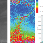
CL microscopy is helpful in revealing the presence and distribution of subsurface crystal defects, such as dislocations and stacking faults, in semiconductor wafers and epitaxial layers. During a measurement, the CL signal shows the local recombination activity of electron-hole pairs and excitons. Additionally, as recombining electron-hole pairs is a competitive process, it reveals non-radiative recombination at electrically active defects as dark contrast in a CL map (see below).
Understanding the electronic structure of crystal defects can prove vital when devising methods to nullify the deleterious effect on device performance. Spectroscopic CL is one of the few methods available to provide a detailed understanding of the distribution, concentration, and energy levels of deep-level states associated with crystal defects. At cryogenic temperatures, non-radiative recombination becomes less probable due to the reduced phonon population, making possible radiative transitions via the defect states. Therefore, spectrally resolved CL can be used to determine the mid-bandgap energy level(s) of defects from the radiative emissions, and the spatial resolution of CL enables measurement of the distribution and concentration of defects.
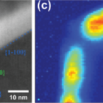
Lifetime and/or minority carrier diffusion
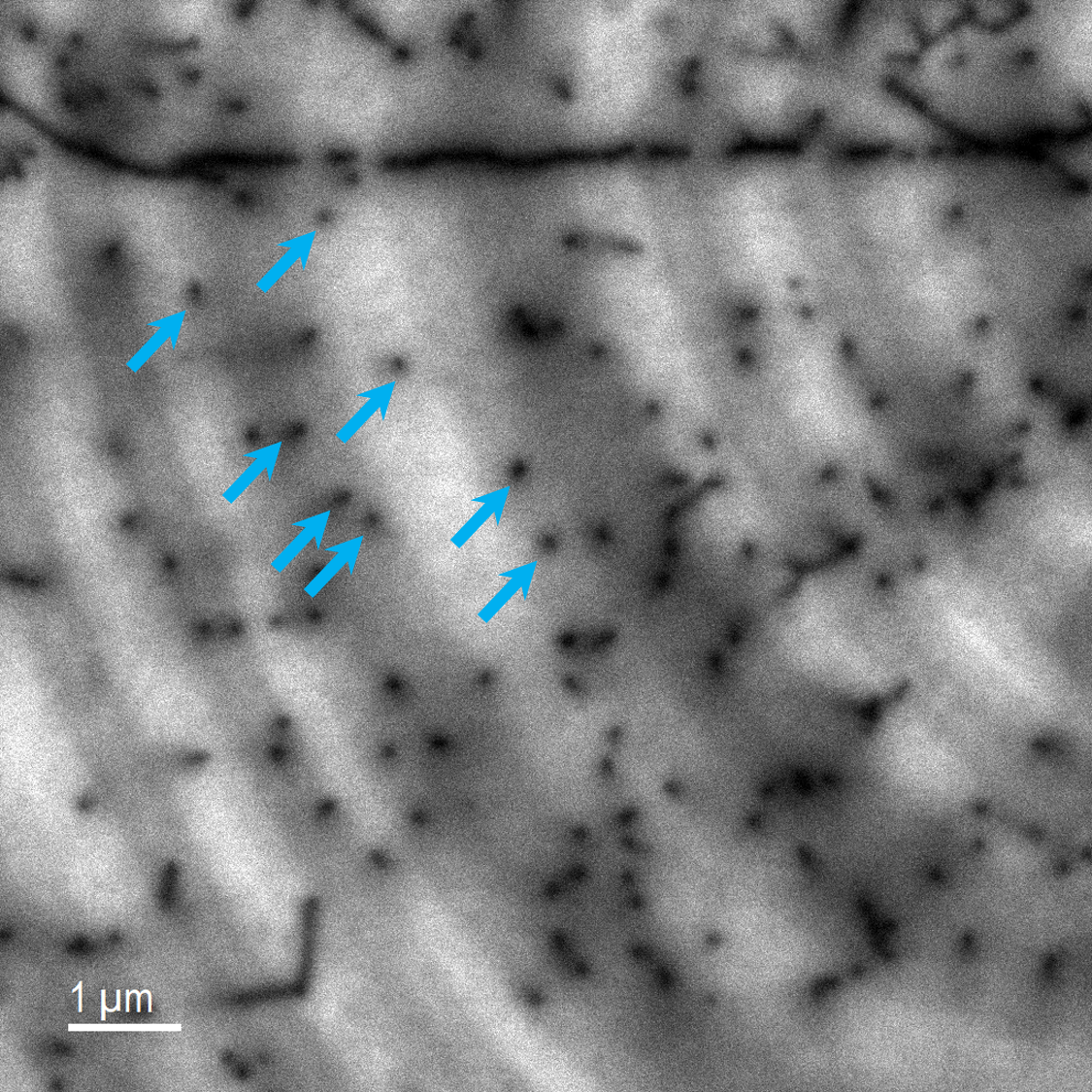
In a semiconductor, the electron beam of the electron microscope generates free electrons and holes. Before recombination, the excess carriers can move within a crystal under drift and/or diffusion mechanisms. Under most experimental conditions, the concentration of these free carriers is far below the majority carrier density concentration of a doped semiconductor, so we typically only need to consider the behavior of the excess minority carriers (or excitons). CL maps may capture this effect so you can observe when the generation volume is small (e.g., at low accelerating voltages): In the CL map of a GaN wafer containing threading dislocations (above), the black dots correspond to an individual threading dislocation intersecting the surface. These defects are one-dimensional, yet the dark spot in the CL map has a diameter >50 nm. This demonstrates that the dislocation impacts the crystal's electrical properties over a more extended range than the dislocation's physical extent or a fraction of the free carriers generated within the minority carrier diffusion length diffuse to the dislocation and recombine non-radiatively. Empirical models are available to extract the minority carrier diffusion length from CL maps of crystal defects. However, recent research demonstrates that time-resolved or spectrally resolved measurements at cryogenic temperatures are superior.
Nanostructure Characterization
The size, shape, composition, and structure of nanostructures are known to modify their functional properties, such as their electrical or optical characteristics. The development of novel devices built from nanostructures depends critically on the ability of scientists and engineers to understand the relationship between structure and function. To this end, electron microscopy and luminescence spectroscopy, or photoluminescence (PL), are commonly employed. Electron microscopy helps determine the size, shape, composition, chemistry, and presence of crystal defects of individual nanostructures at or near-atomic resolution. While PL provides insight into band gap and electronic structure. This approach has demonstrated its usefulness with many highly promising devices close to commercialization. However, the PL technique typically measures the average properties of a nanostructure ensemble, and there is a growing realization that the different spatial resolutions used in the two techniques may lead to unsound conclusions.
Cathodoluminescence is a particularly valuable characterization technique for semiconductor nanostructures, providing the power of optical emission spectroscopy at a spatial resolution that enables individual nanostructures to be investigated and, in some cases, individual quantum wells or discs. Furthermore, the availability of other signals in the electron microscope enables a direct correlation of functional properties with sample structure and composition, often simultaneously.
Experiment briefs and application notes
Device Characterization
Cathodoluminescence (CL) is used widely in optoelectronic device characterization and failure analysis. We already see how CL is a highly beneficial tool for composition metrology and quantification of crystal defects in compound semiconductors, and these analysis methods often extend to fully processed devices in metrology and failure analysis. In the following section, we review the uses of CL in a range of commercial devices.
Light Emitting Diodes
Light-emitting diodes (LEDs) are more efficient, faster, and have a much smaller footprint than filament-based light sources. LEDs are composed of semiconductor materials whose electronic density of states includes a forbidden band known as the band gap. When electrons and holes are excited and allowed to recombine across the band gap in a semiconductor, the emitted photon (observed as light) carries the energy of the band gap. The advent of the blue LED in the 1990s and the subsequently explored tunability of the III-nitride materials paved the way for LED-based lighting and display technologies.
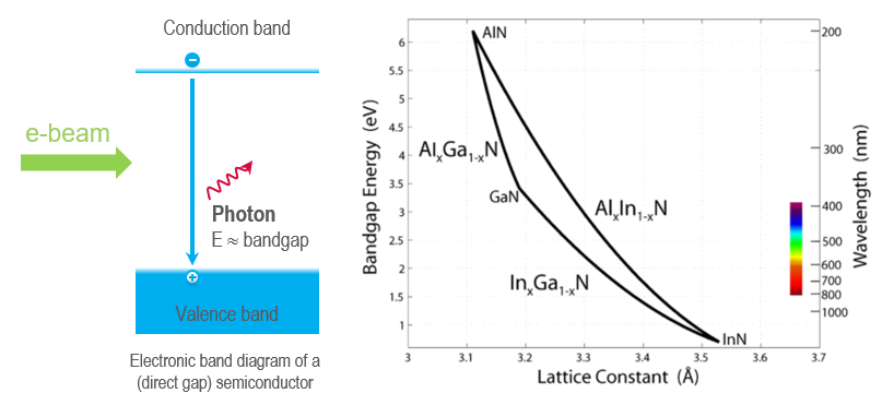
For LED applications, GaN is usually grown in a heterostructure form with a number of InxGa1-xN quantum wells (QWs). These generate efficient light emission in the visible part of the electromagnetic spectrum rather than at the native (GaN) band gap energy of 3.4 eV (365 nm). They are useful for enhancing gain and optical confinement by increasing the active region volume and allowing the tunability of the emission color (wavelength).
The cathodoluminescence (CL) technique is a fast and highly relevant method in the process development of GaN LEDs. The energetic electron beam can effectively excite the wide band gap of nitride semiconductors (even AlN) and provide spatial resolution down to 10 and 1 nm for CL measurements performed in the scanning electron microscope (SEM) and transmission electron microscope (TEM) instruments, respectively. One can directly visualize the distribution of non-radiative defects, such as dislocations, and determine the identity of point defects. Furthermore, the spatial variation of strain, doping, growth direction, and carrier concentration can all be determined, as well as the different constituents of the stack (e.g., AlN, GaNs, quantum wells).
In addition, you can visualize the emission pattern using the angle-resolved or wavelength- and angle-resolved modes of operation. These modes offer another significant metric for light-emitting devices as they enable detailed spectra characterization using angle-resolved CL imaging.
Experiment briefs and application notes
 |
 |
| Cathodoluminescence as a technique for inspection, metrology, and failure analysis of microLED processing | Nano-cathodoluminescence enables the design of light-emitting diodes with higher efficiencies |
3D metrology of an LED structure
While CL provides high-lateral spatial resolution to investigate semiconductor materials, it also enables depth-resolved measurements. Using the selected accelerating voltage of the SEM to determine the surface depth that the CL signal is generated from enables the analysis of layers buried within the bulk material. Furthermore, it allows the investigation of 3D structures by depth-resolved CL spectroscopy, which compares the simulation of primary electron scattering with carrier drift and/or diffusion. Such depth-resolved measurements enable:
- Mapping of the depth and lateral distribution of dislocations and basal plane stacking faults in fully processed devices
- Thickness measurements of sub-surface layers of different compositions, including analysis of individual quantum wells within a multi-quantum well stack
- Location of point defects at specific interfaces within a device structure (with ~1 nm axial resolution)
Failure analysis
General lighting applications and car lights frequently use white and blue LEDs, but their use also penetrates more diverse purposes, including industrial environments. In such environments, the devices are subject to extreme environmental conditions such as mechanical vibrations, or enhanced or extremely low temperatures, humidity, or chemical substances. There is a growing realization that the LED chip itself, rather than a peripheral element, can lead to module failure under these conditions. With such a diverse range of applications, laboratory testing procedures can't replicate all use cases in real field applications. It is, therefore, necessary to use analytical techniques capable of observing the LED structure on a macroscopic and microscopic scale, characterizing both physical structure and functional properties. To this end, electron microscopy, including CL, is an attractive and effective tool in evaluating failure causes in light-emitting devices.
MicroLEDs
MicroLED arrays
Light-emitting diodes (LEDs) are an attractive alternative display technology. LEDs' high emissivity and low power consumption promise significant improvements over existing technologies in augmented reality and mobile device displays. To cover the full-color gamut for displays, LED pixels contain red, blue, and green single LEDs arranged in an array. Hence, the resolution of displays depends on the size and pitch of single LEDs. In efforts to improve resolution by reducing the size of the emitters, the irradiance is consequently reduced. For smaller conventional LEDs to achieve comparable irradiance, they require a higher input power that can lead to more significant heat dissipation requirements.
 |
Cathodoluminescence as a technique for inspection, metrology, and failure analysis of microLED processing |
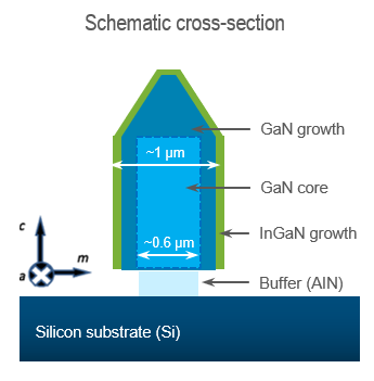 Hexagonal core-shell pillar
To combat the aforementioned issues that use conventional flat emitters, researchers have turned attention to 3D microLEDs (μLEDs). Such emitters have the apparent advantage of increased surface area, where further the increased dimensionality allows for the formation of quantum wells on the sides of the emitter. The increased dimensionality also provides access to various crystal faces. GaN includes the m-plane, which has a minimal native electric field that reduces the influence of the quantum confined stark effect (QCSE), thereby improving the recombination efficiency of excited carriers.
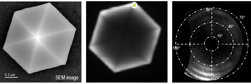
Compositional variation and defects
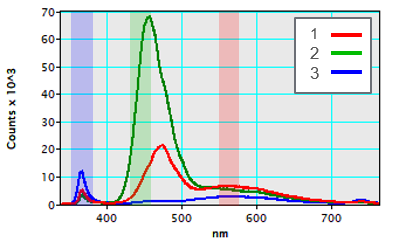
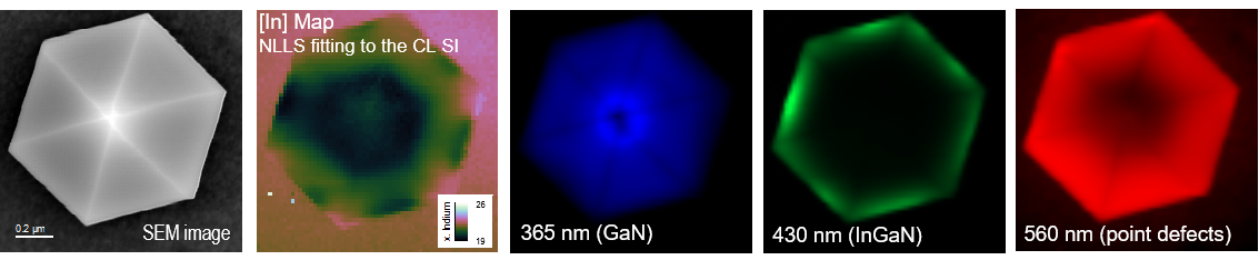
A GaN/InGaN core-shell pillar is a typical 3D emitter. Observing the cathodoluminescence (CL) from such a pillar allows for extracting spectral information as a function of position. Spectral information can be spatially mapped in bands of interest that are readily displayed, e.g., the GaN, InGaN, and point defect bands. Further, in this analysis example, compositional spatial mapping of the InGaN quantum well active layer reveals the In-fraction lies between 19 – 26% and concentrated at the vertices. The native non-linear least squares (NLLS) spectra fitting tool in DigitalMicrograph® software helps estimate the compositional mapping and determine the InGaN band gap as a function of position. The NLLS fitting determined the band gap, which allows for the estimation of In concentration, x, and material composition, which is determined by observing the theoretical band gap of InxGa1-xN as a function of x. Thus far, we have information on spectral CL emissions, but without information concerning the angles of emissions, such shaped specimens can emit anisotropically. To observe such anisotropy, the angle-resolved CL mode of operation can be used.
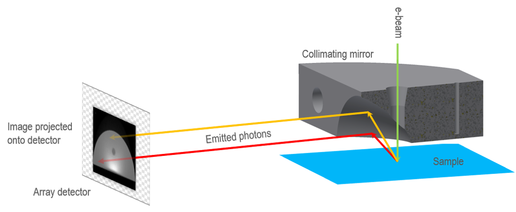
Angle-resolved cathodoluminescence
When light is emitted from a specimen at the focal point of the parabolic mirror, it reflects down the mirror's axis. Mathematically, the paraboloidal shape is 1-to-1. Therefore, the position of the light's reflection on the collimating mirror is unique to the emission angles from the sample. Hence, the angular emission information is acquired by simply imaging the backplane of the paraboloidal collection mirror. With a known mirror shape, you can transform the data into a polar representation for a more straightforward interpretation.
Emission selectivity and shape effects
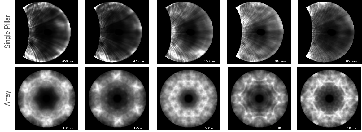
In the case of the single out-of-array microLED pillar, the ARCL revealed an emission selectivity of about 2.4x stronger at ~70˚ compared to the normal direction when integrating the entire pillar. As one might expect, the direction of emission depends on the position of excitation. The emission is most intense in the direction opposite from the side of the pillar, which is excited and includes an interference pattern. The intensity directionality is likely due to the effect of total internal reflection from the index contrast at the pillar surface with vacuum. At the same time, the interference pattern is due to reflections from the sample surface.
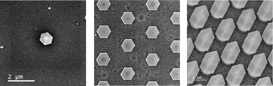
microLED hexagonal pillar array
MicroLEDs are most frequently arranged in an array configuration. In this case, the array configuration is hexagonal with (edge-to-edge) pillar width of ~800 nm and a (nearest neighbor) period of ~2 μm. Such an array using GaN opens the possibility of photonic influences on optical behavior. Therefore, observing them in such an array is essential to determine the impact on light emission.
Effective compositional variation and defects
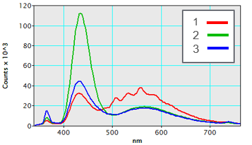
An in-array single pillar was observed using the same data acquisition as the previously displayed out-of-array pillar. Again, we observe the spectrum for every point scanned in this spectrum image, which allows for emission band mapping of the GaN, InGaN, and point defect bands and estimation of In content by position across the pillar surface. Here, we see an estimate of indium content in InxGa1-xN of between 11 and 19%.
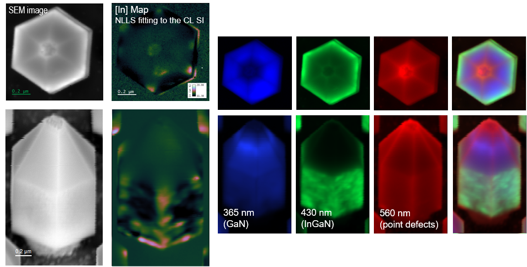
Several interesting observations can be made in this comparison of in- vs. out-of-array microLED pillars. In the out-of-array device, the overall intensity comes from the edge, as expected, since the quantum well is excited directly. Meanwhile, the intensity is more evenly distributed across the surface of the in-array device. Observing spectra from various positions further reveals an enhancement in the overall intensity of the in-array device, especially in the 500 – 600 nm range where multiple smaller peaks are present. The differences are perhaps even more obviated by the color band images of the GaN, InGaN, and point defect bands. In these images, the array influence produces very different emission maps for each excitation position.
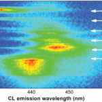
Once the array's influence on light generation is understood, it is common to explore the emission anisotropy as a function of wavelength to determine whether a microLED is feasible for implementation in a display device. To do this, we employ the wavelength- and angle-resolved CL (WARCL) technique, including wavelength information and angular. This reveals any preferential direction of emission and allows for the observation of photonic bandgaps.
Here is a side-by-side comparison of WARCL frames at several wavelengths. The weaker emission in the direction normal to the pillar is present in the out- and in-array LEDs. However, an interesting behavior is present for the in-array, demonstrating the usefulness of the WARCL technique for microLED arrays.
Further information on the photonic crystal behavior of micro-pillar arrays can be found here.
Application Note
Laser Diodes
Aging studies and failure analysis of laser diodes
Semiconductor lasers are important for many applications, such as material processing, medical surgery, pumping of solid-state and fiber lasers, and space applications. Many of these applications require high reliability and predictability of lifetime due to the expense and/or difficulties in accessing their installation locations in environments like undersea fiber cables or satellite laser terminals.
Cathodoluminescence (CL) analysis is useful for revealing defects that nucleate during a laser diode's useful life, how these evolve under further operation, and the type and location of defects that can lead to device failure.
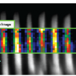
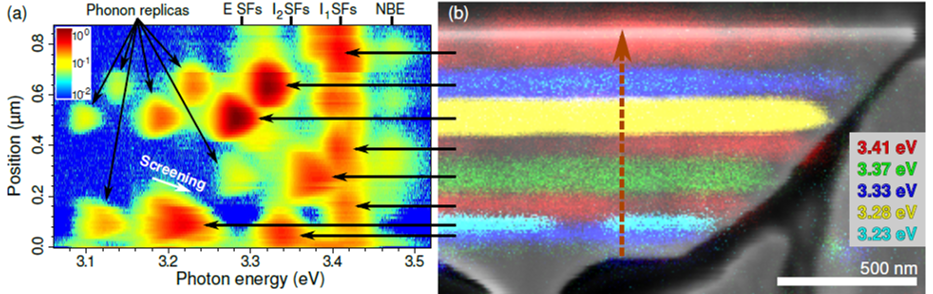
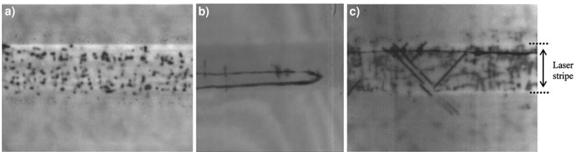
For example, CL images of three different broad-area laser diodes (50 µm stripe width and 1.5 mm resonator length) at different stages of lifetime testing are shown below. The laser diodes comprise a GaAsP/AlGaAs single quantum well embedded in a 2 µm thick AlGaAs waveguide structure. The images show example images of laser diodes that exhibit (a) gradual degradation, (b) freak (early) failure, and (c) sudden failure after gradual degradation. During extended lifetime testing, an increasing concentration of dark spots can be observed from a CL image (e.g., images a and c). The dark spot contrast originates from newly nucleated dislocation loops, and the dislocation loop concentration correlates well with a gradual degradation in device performance, e.g., the need for higher drive currents to maintain a constant output power. However, while laser diodes exhibit only these dark spots, catastrophic failure is avoided. Dark lines can be observed through the laser stripe in devices that exhibited catastrophic failures (b and c). These dark lines are extended dislocations formed by glide and climb processes of dislocation loops. The suddenly failed device (c) indicates dark lines running in [110] along the laser stripe and in [100] directions, the latter inclined 45° towards the laser stripe.
Photovoltaics
Photovoltaic (PV) materials and devices play a crucial role in our fight to reduce human-made greenhouse gas emissions. However, fossil fuel-derived electricity is still cheaper to produce (typically) than electricity from renewable sources like PV. To make (or, in some cases, keep) renewable electricity cost-competitive with fossil fuel electricity, we must continue to improve PV and other renewable technologies.
Cathodoluminescence (CL) is useful for revealing the microscopic mechanisms that determine the macroscopic performance of PV devices and modules. This allows researchers to understand and analyze fundamental physical and chemical processes in materials such as thin-film, perovskite, silicon, and other semiconductors; industrial applications include quality control and failure analysis.
Thin-film Multi-crystalline silicon
Perovskites
Despite only recently becoming an intense research focus, halide perovskite solar cells achieve exceptional efficiencies that surpass thin-film PV materials like CdTe and CuInGaSe2. They exhibit high carrier mobility, long diffusion lengths, and tunable spectral absorption windows. As a result, many researchers claim halide perovskites have the potential to be the most extraordinary and market-competitive optoelectronic material. With that in mind, significant hurdles remain to mainstream adoption, and researchers will require characterization techniques capable of exposing the interplay among structure, chemistry, and optoelectronic properties to inform processing strategies to increase device efficiencies and long‐term stability.
CL microscopy is an ideal technique for providing this type of information due to its ability to capture high spatial resolution and robust optical and electronic information. CL can monitor degradation due to environmental factors, reveal phase segregation resulting from material processing, and address other halide perovskite‐centric material issues.
It was once thought that electron beam‐based analysis of halide perovskites was impractical due to the instability of material properties when exposed to high-energy electrons. However, recent developments have stabilized formulations and refined optical designs for high sensitivity and repeatability, making analysis below the damage threshold for many halide perovskites possible.
Experimental brief
 |
Revealing the spatial distribution of phases in perovskite solar cells for the development of high efficiency and stable devices |
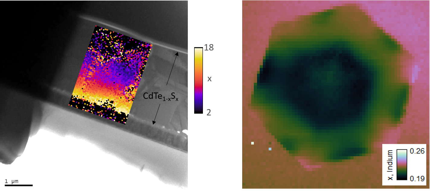
Thin-film
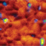
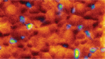
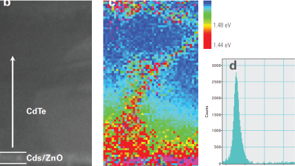
Thin-film solar cells based on CdTe or CIGS are the leading PV technology widely commercialized. Further improvements to device and module efficiencies require increased minority-carrier lifetime within the CdTe absorber layer. The low minority-carrier lifetime in polycrystalline thin films is thought to be caused by non-radiative Shockley-Read-Hall (SRH) recombination at deep levels in the band gap created by crystal defects—both point defects and extended defects are known to be prevalent in thin-film solar cells. However, there has been a failure to reach a consensus on precisely which defect(s) is(are) most limiting with the ongoing debate surrounding the role of grain boundaries after thermal processing. To this end, cathodoluminescence (CL) is an important technique that enables researchers to analyze recombination processes at the defect scale, allowing macroscale device performance to be understood from the microscopic behavior.
Many researchers use the nano-scale spatial resolution of CL to qualitatively and quantitatively compare carrier recombination and defects at grain boundaries and interiors before and after treatments designed to passivate defects. The contrast in a CL map of a polycrystalline material reveals regions of the specimen with strong(er) non-radiative SRH recombination, often grain boundaries. Statistical analysis and correlation using grain boundaries (e.g., EBSD analysis) provide a quantitative understanding of recombination at grain interiors and a variety of grain boundary types. Recently, CL measurements also allowed researchers to determine the grain boundary recombination velocity. Furthermore, capturing a complete CL spectrum at every (spatial) pixel in a map (spectrum imaging or hyperspectral imaging) allows researchers to map compositional variation within the compound semiconductor grain interiors and to develop more accurate band model diagrams to model carrier behavior.
Experimental brief
 |
Mapping the electronic bandgap of semiconductor compounds with milli-electron volt accuracy |
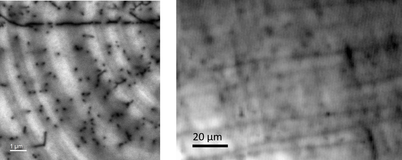
Multi-crystalline silicon
Silicon has an indirect electronic band structure. Since this band-to-band radiative recombination has only a low probability in comparison to non-radiative transitions at room temperature, it makes CL largely impractical. However, CL is useful for measuring the luminescence behavior of extended defects at cryogenic temperatures. These valuable measurements can simultaneously obtain spectrally and spatially resolved information to provide deep insights into the electronic structure of extended defects. For example, defects include dislocations and grain boundaries, which control the performance of many electronic and photovoltaic devices.
In many CL experiments, extended defects act as non-radiative recombination centers, and, therefore, the luminescence from band-band-recombination is decreased in the vicinity of extended defects compared to the undisturbed semiconductor. In the case of Si, Ge, and some compound semiconductor materials, dislocations and grain boundaries can exhibit characteristic luminescence bands (with photon energies lower than the band gap) that reveal the detailed electronic structure of defects. This allows researchers to develop accurate recombination models to improve device performance. Extensive CL investigations of bonded silicon wafers and multi-crystalline silicon show that dislocations and low-angle grain boundaries are responsible for the occurrence of shallow and deep levels in the band gap—the radiative transitions associated with these defect states are denoted as D-lines (D1 – D4). There remains ambiguity over the role of the strain field accompanying extended defects and oxygen and transition metal contamination. The correlation of the information revealed by CL with other techniques in the SEM, such as EBSD, shows strong promise as a means to resolve uncertainties and provide manufacturers guidance in optimizing materials and device processing.