Getting Ready
Learn about the important parameters to optimize each cathodoluminescence (CL) experiment, including sample preparation, electron microscope setup, technique selection, and alignment considerations. Understanding the effect of these key parameters will help ensure a successful CL experiment and improve the quality of your analysis.
Sample Preparation
Cathodoluminescence (CL) microscopy can be performed in the scanning (SEM) or transmission electron microscope (TEM), and—as with other forms of microscopy—the requirements for sample preparation vary significantly. Experiments in the SEM allow analysis for a broader range of sample types, including bulk specimens, 6" wafers, packaged devices, thin geological sections, epoxy mounts, and nanoparticles dispersed on a supportive substrate. Meanwhile, the TEM requires thinning specimens to electron transparency to attain a potentially higher spatial resolution.
SEM
CL analysis often requires little or no sample preparation beyond that needed for general SEM imaging and analysis. Samples should be macroscopically flat and free from sample preparation-induced defects, e.g., scratches from mechanical polishing or ion-induced defects from focused ion beam (FIB) sample preparation methods. We recommend a clean-up step for FIB-prepared specimens using broad argon beam milling, such as the PECS™ II or Ilion™ II system.
Many samples of interest are insulators or wide band gap semiconductors. For these materials, it may be necessary to coat the sample's surface with a conductive layer to prevent charge accumulation. For this purpose, a thin 1 – 3 nm carbon layer is preferred over metal evaporation due to the low and uniform absorption of the light escaping from the specimen. Analysis in an environmental or low-vacuum SEM chamber may be possible. However, some gases (e.g., water vapor) provide a background luminescence signature that may obscure the luminescence signal.
CL in the SEM does allow the analysis of sub-surface features by providing the freedom to control the penetration depth of the incident electron beam. The accelerating voltage of the SEM determines the depth below the surface and, depending on the sample, extends the analysis range up to 5 – 10 μm. For this analysis, the interaction volume created by the electron beam must be able to access the region of interest. Some semiconductor devices may limit analysis to specific sample geometries or require a small degree of sample processing.
When using detection systems that use a light-collection mirror, the sample's region of interest must be located at the focal point of the collection mirror. The Monarc® and ChromaCL™ systems allow for 1 mm clearance between the sample and mirror and accommodate 6" and 3" diameter samples, respectively. Additionally, the Monarc supports sample tilts of 25° (in a single axis).
In many nanophotonic applications, surface plasmon polaritons are only supported at metal-dielectric interfaces (e.g., metal-vacuum surface); any hydrocarbon contamination can dampen the optical response and provide misleading results. We strongly recommend using a plasma cleaner (e.g., Solarus® II) to prepare contamination-free surfaces for optimum results.
TEM
CL requires little or no sample preparation beyond what is necessary for general TEM imaging and analysis. We recommend using an argon-milling system like the PIPS™ II to clean up FIB-prepared specimens and remove gallium-induced defects. We also recommend plasma cleaning using a Solarus II plasma cleaner or similar system. In many specimens, the low intensity of the CL signal necessitates large probe currents, consequently leading to a higher rate of hydrocarbon contamination.
When preparing semiconductor devices and materials, note that as the sample becomes thinner, the effect of surface recombination becomes increasingly important. In cases where the sample is thinner than the minority carrier diffusion length, surface recombination may quench the emission entirely. The effect may be less severe for semiconductor samples that contain heterostructures and other nanoscale features, as the band gap alignment is often designed to prevent surface recombination.
In many nanophotonic applications, surface plasmon polaritons are only supported at metal-dielectric interfaces (e.g., metal-vacuum surface); any hydrocarbon contamination can dampen the optical response and provide misleading results. We strongly recommend using a plasma cleaner (e.g., Solarus® II) to prepare contamination-free surfaces for optimum results.
Sample's contribution to image drift
Common environmental factors can cause your sample to drift during an experiment, including vibration, thermal variations, and stray electromagnetic fields. This drift may cause image blurring that impacts the resolution and quality of your data. Below are frequently encountered sources of drift related to the sample itself:
-
Charging
-
Symptoms – Sample drift or jumping will increase as higher probe currents are applied
-
Solution – Coat your sample with carbon to make the sample conductive
-
-
Improper sample mounting
-
Symptoms – Sample vibrates
-
Solution – Verify how securely fastened the sample is to the grid or holder
-
Microscope Setup
The practicalities of preparing for a cathodoluminescence (CL) experiment vary between a scanning electron microscope (SEM) and a transmission electron microscope (TEM). Please refer to the appropriate section below.
SEM
To get ready to perform a CL experiment, please take the following steps:
-
Secure the sample to a stub suitable for the SEM; for insulating specimens, ensure the sample surface has a good electrical path to the SEM stage.
-
Insert your sample into the microscope chamber.
-
Set the electron microscope to the desired analysis conditions (refer to specimen-dependent recommendations).
-
Find the region of interest you want to investigate.
-
Insert the collection mirror after ensuring that it is safe, e.g., that the sample (or another detector) does not occupy the space that the CL mirror occupies.
-
Turn the electron beam on and perform a basic alignment of the electron column.
-
Align the CL detector and sample; this step is critical to achieving the highest-quality CL results (see the Alignment section).
-
Perform final alignment of the electron microscope to help maximize image brightness and minimize image distortions.
Selecting the best SEM settings
How a user sets up the microscope is particularly important when considering CL experiments. The selection of the optimum operating parameters, such as accelerating voltage and probe current, is highly dependent on the sample(s) for analysis.
The table below provides guidance for a range of specimens. To learn why and how to optimize these settings for your specimen(s), please refer to the optimization discussion in the Mapping, Spectroscopy, and Emission Pattern portions of the How To section.
| Sample type | Strategy for sharper images | Possible limiting factors | Typical accelerating voltage (kV) | Typical beam currents (nA) |
|---|---|---|---|---|
| Insulators | Lower accelerating voltages |
|
5 – 20 | 1 – 100 |
| Semiconductors, direct band gap | Lowest accelerating voltage |
|
0.5 – 10 | 0.001 – 20 |
| Semiconductors, indirect band gap | Lowest accelerating voltage |
|
5 – 30 | 1 – 100 |
| Metals | Higher accelerating voltages |
|
20 – 30 | 0.1 – 20 |
TEM
Before you start an experiment, the TEM must be well aligned. Perform the emitter, condenser, and optic axis adjustments typical for your TEM; this will help maximize image brightness and minimize lens aberrations.
It is important to note that the CL results that you can obtain will depend on your sample type and the accelerating voltage selected. The table below suggests TEM operating conditions for a range of specimens.
| Sample type | Possible limiting factors | Typical accelerating voltage (kV) |
|---|---|---|
| Insulators |
|
40 – 120 |
| Semiconductors, direct band gap |
|
40 – 80 |
| Semiconductors, indirect band gap |
|
40 – 80 |
| Metals |
|
200 – 300 |
To get ready to perform a CL experiment, please follow the below steps:
-
Set the TEM to the desired accelerating voltage for your specimen.
-
Load the sample into the Vulcan® holder.
-
Set the sample so the region of interest is within the lateral focal range of the Vulcan holder's optics. This step is critical to achieving the highest-quality CL results (see the Alignment section).
-
Plasma clean your sample using a Solarus® II plasma cleaner or similar system.
-
Insert your sample into the column.
-
Find the region of interest you want to investigate.
-
Set the TEM to an eucentric focus value and bring the sample to the eucentric height.
-
Insert and align the hard x-ray aperture (some TEMs only).
-
Set the TEM to scanning (STEM) mode.
-
Perform the electron microscope's final alignment, as the aperture in the collection mirrors may have disturbed the optimum alignment conditions.
Alignment
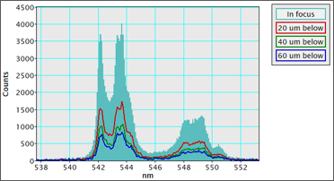
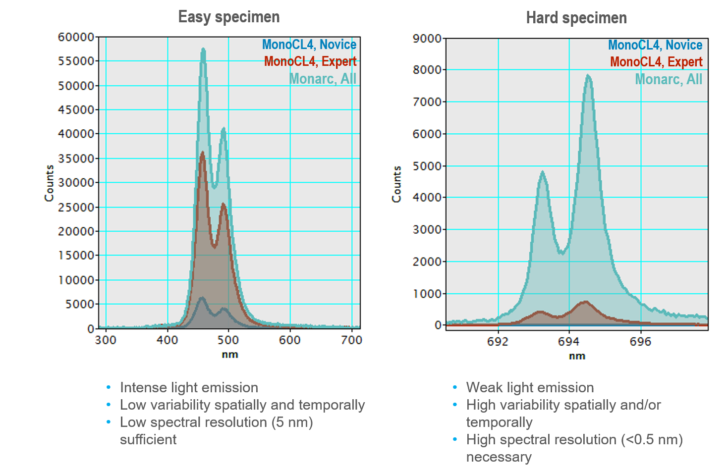
Anyone who has used an electron microscope or looked down an optical microscope realizes the ability to align and focus the (electron) optical system is critical to achieving the sharpest images. Cathodoluminescence (CL) microscopy experiments use both the electron optics of the scanning (transmission) electron microscope (SEM or STEM) and the light optics of the CL detector, and each must be aligned well. The two optical systems and samples must be co-aligned precisely to collect the sharpest CL maps, spectra, and emission patterns. As seen in the example spectrum (collected with the Monarc® system), misalignment of as few as tens of microns in a single axis significantly reduces performance. In other CL systems, a misalignment of just a few micrometers can prevent meaningful data from being collected.
In the following section, learn why optical alignments are so important and how to adjust a system to capture the best results. The system includes independent methods for Monarc users that automatically perform the alignment step without user input. The following section is useful for developing understanding, but proceed to the Monarc system's instructions for the practicalities of collecting optimized results.
SEM
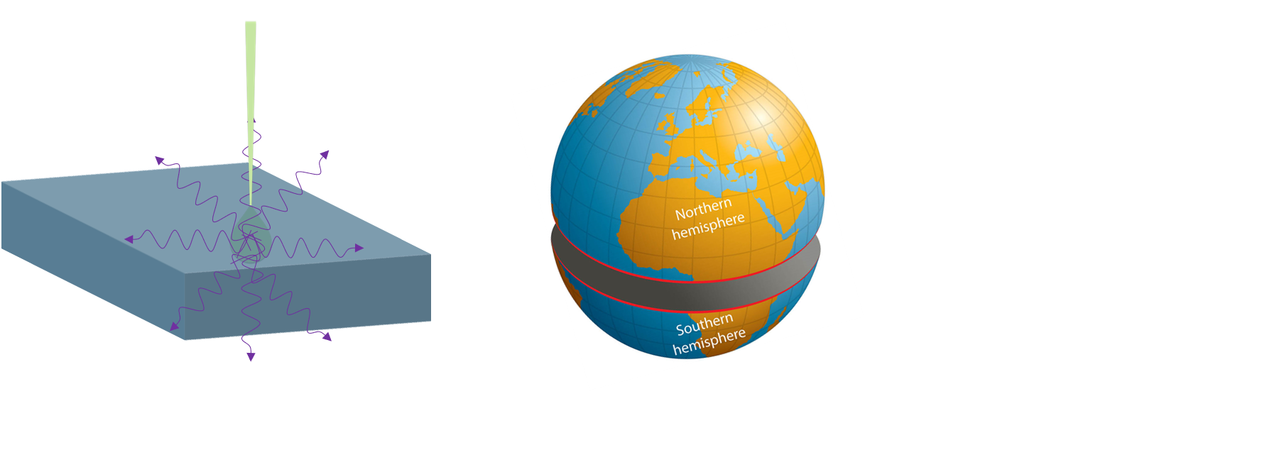
The electron beam generates light within our sample, e.g., within the interaction volume. In many specimens, these photons radiate isotropically, e.g., propagate with equal intensity in all directions. It may help to visualize this process by considering the light emission as a point source located at the center of the globe that radiates such that there is equal illumination at all points on the surface of the globe:
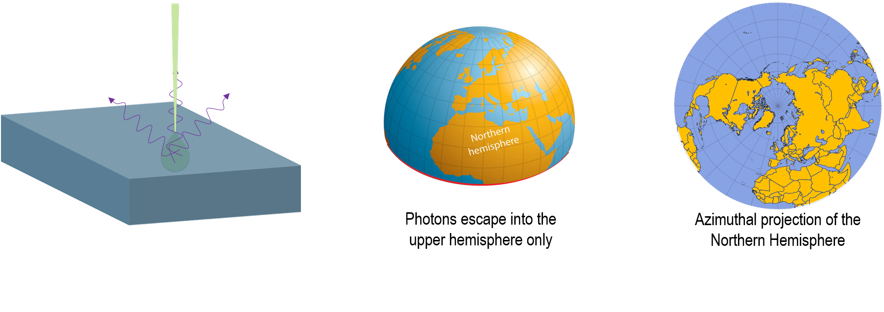
In some cases, the sample may absorb light before it ever escapes the specimen before it reflects and refracts at the sample's surface and is absorbed by the electron microscope stage or holder. For these reasons, in bulk specimens, it is more typical to consider that photons are emitted from the sample surface into the upper hemisphere only:
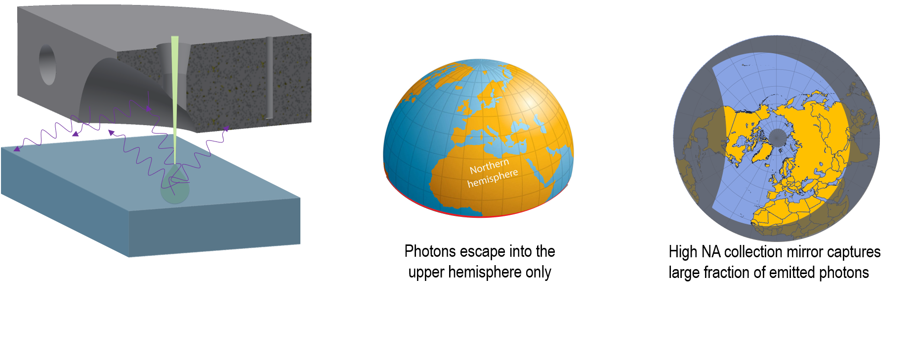
To have a detector with high sensitivity, it is of utmost importance to maximize the collection of photons. The preferred method is to use a high–NA (numerical aperture) collection mirror. A typical collection mirror is an off-axis paraboloid with an aperture to allow the electron beam to reach the specimen. When the sample is located at the parabola's focal point, ~85% of the emitted photons are collected and reflected into a collimated beam for further processing by an optical system. The polar plot of the Northern Hemisphere below illustrates the solid angle covered by a typical collection mirror:
In these high-sensitivity systems, optical alignment becomes critical to capturing sharp maps, high-resolution spectra, and emission patterns. See, for example, comparative CL maps and a collection of spectra captured with varying degrees of misalignment in (just) one axis below:
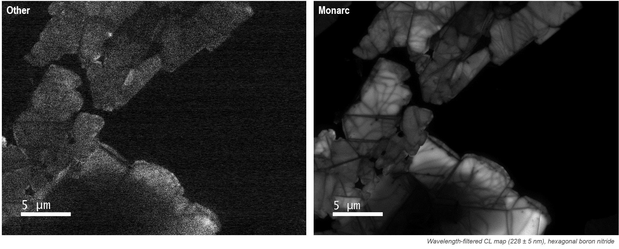
In these unfiltered CL maps of hexagonal boron nitride, a misalignment of 100 μm (in the Z-axis) reduces the signal-to-noise ratio by a factor of 10, but with poor alignment in more than one axis, this could easily be a factor over 1000.
In the example of a CL spectrum shown at the top of the page, a 20 μm misalignment in the Z-axis reduces the collected signal by 50%, and at a misalignment of 60 μm, you can no longer resolve the double peak at 543 nm. In some analysis systems, a misalignment of just 5 μm may prevent data collection.
Basic alignment workflow
The basic steps to begin using a high-performance, mirror-based CL system appear to be straightforward:
-
Insert the collection mirror.
-
Center the collection mirror.
-
Set the sample at the operating working distance.
-
Focus on the SEM image.
-
Start your experiment.
We have already seen that it is important to align the SEM, CL system, and sample to within only a few micrometers. This sounds challenging enough, even before considering that you cannot directly observe the focal point of the collection mirror. The collection mirror of a CL system is designed with an aperture to allow the electron beam to reach the sample. Thus, the CL mirror's focal point is approximately at the center of the aperture. However, the exact location depends not only on the accuracy of the mirror itself but also on the alignment of the SEM's electron beam. When the SEM's accelerating voltage changes, the electron beam axis can shift, causing an apparent translation to the mirror's position and, if the optical axis of the SEM is not perpendicular, an apparent shift in the position of the focal point within the aperture.
With a specimen that emits light strongly and uniformly over hundreds of microns, performing this alignment manually after good operator training is relatively straightforward. Most, if not all, samples of interest for CL measurements exhibit significant spatial variation that makes this challenging or impossible even for expert users on many specimens.
Monarc MonoCL™/ChromaCL™ Vulcan®
Schematic ray diagram
As we have seen, optical alignment is critical to collect optimal results (sharpest images or spectra or during the shortest acquisition time). In the following section, a simplified ray-trace diagram helps explain why alignment is so critical to many of the basic modes of operation of a CL system. One consequence of employing a collection mirror is that the alignment of the sample, the electron beam of the SEM, and the CL system becomes very important. Consider the simplified schematic of a CL detector shown below:
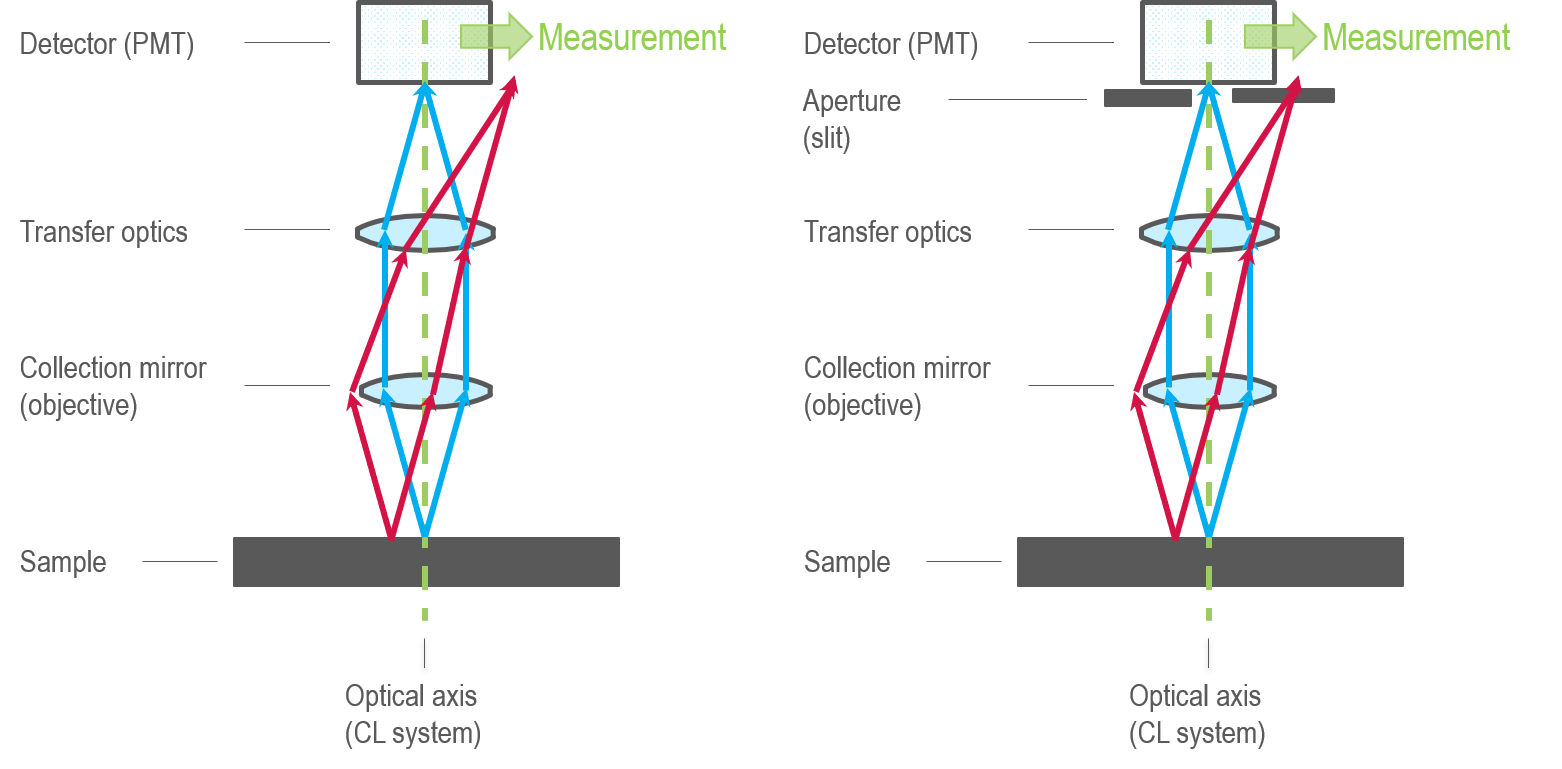
One can assume that light emerges from the sample at the location of the electron beam. If the sample and CL system are aligned well (blue lines), the light reflects from the collection mirror in a collimated ray bundle. For instance, the light rays travel parallel to transfer optics (a generalized term for the lenses, mirrors, or optical fibers used in the optical design). This transforms the ray bundle into a format suitable for the downstream analysis hardware. If the two systems are not aligned well around the CL system's focal point (red lines), the ray bundle no longer travels through the optical system in the intended manner, and few photons reach the downstream analysis hardware. This is even more critical when the light bundle must travel through an aperture, e.g., the entrance slit to a spectrograph, before reaching the detector. This has some important consequences:
- High fluence only when the sample is located at the CL system's focal point
- Low fluence when the beam is scanned out of the focal range of the optical system (vignetting) – A limited field of view in CL maps
- The field of view to capture CL spectra depends on the spectrograph's slit width unless you employ special transfer optics are employed (e.g., in the Monarc models 450 and 450.FS)
- Alignment must be sufficiently good not to destroy angular information in the image projected from the collecting mirror
TEM
The electron beam of a transmission electron microscope (TEM) generates light from within a sample. In many specimens, the photons radiate isotropically, e.g., propagate with equal intensity in all directions. The most efficient way to collect these emitted photons is to use large solid-angle mirrors positioned above and below the specimen, as in the holder of the Vulcan system. Light reflects from the mirrors and focuses on optical fibers that run out of the microscope to detect the hardware.
Proper optical alignment is critical in mirror-based systems. For example, a misalignment of just a few tens of micrometers can reduce the signal by 50% or more. With samples in the TEM typically emitting only weakly, precise optical alignment of a sample to the collection system is challenging and fraught with danger in the hands of inexperienced users unless, as with the Vulcan system, the system design guarantees optical alignment in most specimens.
Alignment for Monarc
The Monarc® detector includes AutoAlign routines that align the Monarc system and sample to the electron beam of the scanning electron microscope (SEM) without needing user input or the sample to be luminescent. The AutoAlign routine provides superior performance for all users, no matter their expertise level.
Insert the collection mirror
To begin, insert the Monarc's collection mirror into the SEM chamber. This occurs when you select the Insert radio button in the Monarc Setup palette in the Microscope tab on the left-hand side of the screen; the mirror will insert in under 10 s.
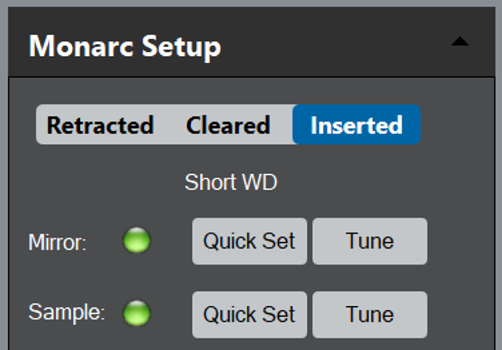 The mirror can be set in one of three pre-defined locations:
- Inserted – Sets the mirror under the pole piece in the cathodoluminescence (CL) operating location
- Retracted – Removes the mirror from the SEM chamber (up to 200 mm)
- Cleared – Partially retracts the mirror to provide a line of sight from the specimen to other detectors
When you insert the mirror at the start of a session, it returns to the last known good position for the current SEM settings.
Center the collection mirror
To align the CL system to the SEM's electron beam, localize the mirror focal point at the center of the SEM field of view. The precise location of this is difficult to determine as the focal point of the collection mirror cannot be observed directly.
Collection mirrors are designed with an aperture to allow the electron beam to reach the sample, and the focal point is located at the approximate center of the aperture. The exact location depends not only on the accuracy of the mirror itself but also on the alignment of the SEM's electron beam. When the SEM's accelerating voltage changes, the electron beam axis can shift, causing an apparent translation to the mirror's position and, if the optical axis of the SEM is not perpendicular, an apparent shift in the position of the focal point within the aperture.
The Monarc system includes a software routine to align the Monarc system to the electron beam axis of the SEM, tracking the settings of the SEM to alert the user when the mirror position may need to be reset.
Two ways of automatically positioning the mirror are available within the software:
- QuickSet – Returns the system to a previously good alignment for that SEM setting
- Tune – Forces the system to revalidate the alignment
The tuning procedure can take a few minutes but need only be applied infrequently during a session. For advanced users, the user may manually position the mirror and store the new coordinates.
Setting the sample at the correct position
For the CL system to operate efficiently, the sample must be set to the focal point of the collection mirror by adjusting the SEM stage location (Z-axis). The Monarc system includes automated alignment routines to optimize the sensitivity of the system uses the Sample alignment in the Monarc Setup palette:
- QuickSet – Returns the system to a previously good alignment for that SEM setting
- Tune – Forces the system to revalidate the alignment
The tuning procedure can take several minutes but need only be applied infrequently during a session.
Tracking the alignment status
The Monarc system tracks the state of the Mirror and Sample alignments, indicating this to the user by a traffic light system:
- Green – Indicates that the system is aligned
- Orange – The system has changed from the known-aligned condition, and alignment may need updating
- Red – No alignment has been performed
Ready to go…
When all components are aligned optimally, the light reflected from the collection mirror forms a collimated beam bundle that is free space coupled to the optical components downstream. The alignment of the downstream optical components is optimized for a collimated beam. No user alignment of the optics is required. For power users, manual control of the mirror position and stored QuickSet locations are available through the setup icon in the Monarc Setup palette.
Alignment for MonoCL and ChromaCL
Insert the collection mirror
To use the MonoCL™ or ChromaCL™ systems, insert the collection mirror into the scanning electron microscope (SEM) chamber manually:
-
Ensure it is safe to insert the collection mirror; the sample should be at a safe working distance, and no other detector should occupy the space needed for the collection mirror.
-
Set the SEM to a magnification of ~100x.
-
While viewing a secondary electron image, slowly insert the collection mirror so that its electron beam aperture appears central in the image.
Set the sample at the correct working distance
 For the cathodoluminescence (CL) system to operate efficiently, adjust the SEM stage location (Z-axis) so the sample is set to the focal point of the collection mirror.
- MonoCL and ChromaCL systems – Refer to the user guide to manually perform this operation.
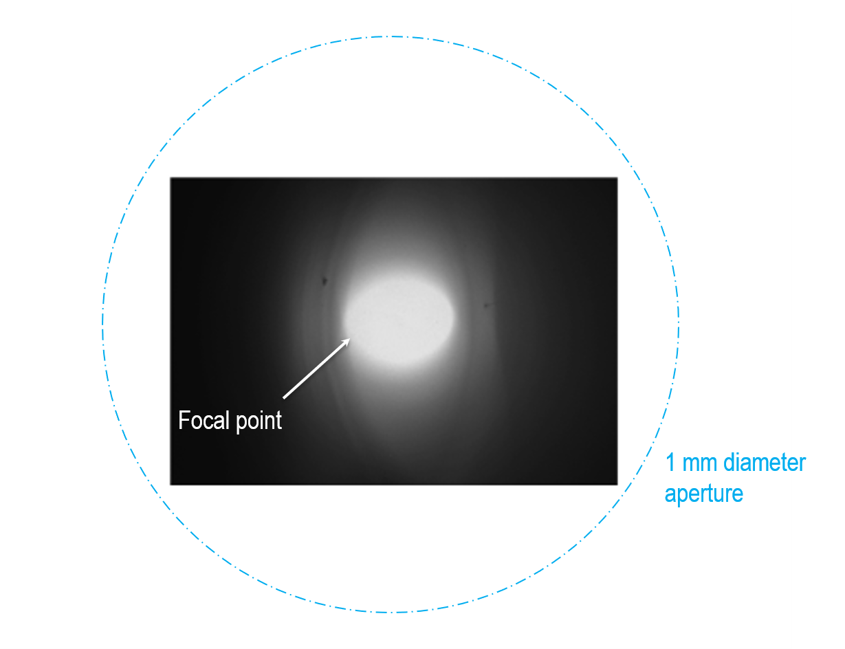
- Systems using the standard 10 mm tall collection mirror – The optimum distance is 0.95 – 1.05 mm below the bottom surface of the mirror. It may require fine adjustment to optimize the position based on the feedback from the CL signal.
The image shows the optimum settings when observing a clearly defined optical focus (hot spot or sweet spot). Note that the focus spot appears more like a crescent when the sample is not at the focal position.
Center the collection mirror
To align the CL system to the SEM's electron beam, locate the mirror focal point at the center of the SEM field of view. The precise location of this can be challenging to determine and track as you cannot directly observe the focal point of the collection mirror. However, you may use the hot spot (see above) and adjust the mirror's position (in the x- and y-axis) to align the hot spot to the center electron beam scan (center of the image). Note that using an electronic image shift will cause an apparent shift in the mirror position. This is useful for fine alignment of the collection mirror but should not be used during CL analysis in case of inadvertent misalignment of the CL and SEM systems.
Ready to go…
When all components are optimally aligned, the light reflected from the collection mirror forms a collimated beam bundle that is free space coupled to the optical components downstream. The alignment of the downstream optical components is optimal for a collimated beam. No user alignment of the optics is required.
Alignment for Vulcan
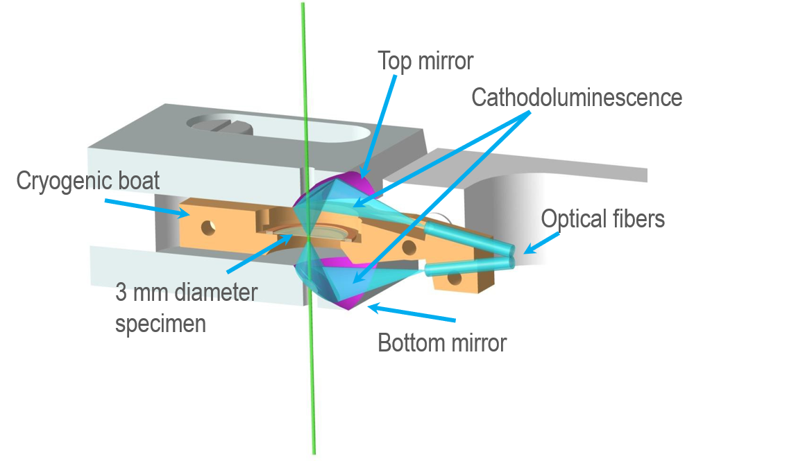
To collect the cathodoluminescence (CL) emitted from a sample, high numerical aperture (NA) mirrors are positioned above and below the specimen. Each mirror contains a small aperture that allows the primary electron beam to excite the specimen and for transmitted electrons to escape. Photons emitted from within a focal point of the collection mirrors are reflected and focused onto optical fibers that carry the signal out of the transmission electron microscope (TEM) column to analysis instrumentation.
A screw ring clamps the sample (3 mm diameter grid) into a small cradle to ensure it achieves good thermal contact.
The cathodoluminescence collection mirrors
The CL collection mirrors are manufactured to a precise mathematical form and are ellipsoidal. Ellipses are defined mathematical shapes with two focal points: one at the sample region of interest and the other at the optical fiber facet. The alignment of the two mirrors ensures each focus is co-aligned to be at the sample's region of interest. The light emitted from the mirror's focal point on the specimen is coupled very efficiently into the optical fibers.
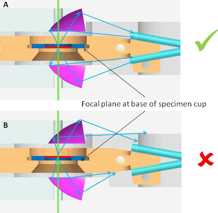
You cannot adjust the CL collection mirrors to optimize the position at which light is collected efficiently from a sample because it degrades light coupling to the optical fibers. The only way to achieve this is by moving the specimen grid within the specimen cradle so that the region of interest coincides with the region from which CL is collected efficiently. An optical microscope and lightbox are available so that you can inspect this during the sample insertion into the sample cradle.
It is important to manufacture specimens so that the thin region of the specimen is approximately centered on the 3 mm grid. For thick samples or a non-standard 3 mm copper grid (e.g., silicon nitride membranes supported on silicon), it is essential to position the sample's region of interest within the focal depth of the system since there is a limited focal depth (z-direction). The focal plane of the mirrors is designed to be the face on which a thin specimen sits. Ensure that the orientation of thick specimens is such that the region of interest is placed against the bottom of the specimen cup. See Figure below.
Technique Selection
During the planning phase of each experiment, it is important to establish what questions you want to answer. When combined with information you already know, such as your sample's geometry or approximate composition, it is easier to select an appropriate technique that delivers answers in the shortest time possible.
 Unfiltered images/maps – Reveal crystal texture in mineralogy, differentiate phases, and quantify extended defects based on their radiative efficiency in semiconductor materials and devices
 Individual spectra from a few well-chosen points – Will typically give the highest-quality spectral data
 Wavelength-filtered imaging – A powerful technique to image one wavelength range (band pass) to determine the spatial distribution of different phases or defects
- Wavelength spectrum imaging – Allows deconvolution of overlapping peaks and mapping of systematic changes in the emission spectrum; collects a complete spectrum at each point in an image
- Individual emission patterns – Determine the direction of photon emission from a few well-chosen points
 Spectroscopic analysis of emission pattern – Capture and analyze the emission spectrum emitted in a given direction or reconstruct emission patterns at a specific wavelength band
- Polarization – Ascertain the polarization state of the light emitted; can be used in conjunction with other modes of analysis